IBM3009K2672
IBM SONET/SDH Framer
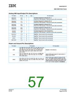
Analog SIM Input/Output Pin Descriptions
Pin Name
Pin No.
I/O
Type
Pin Description
On-Board Capacitor for Receive PLL 1:
Reserved for test purposes. These pins must be left unconnected.
RXCAP1P
RXCAP1N
G17
G18
I
I
On-Board Capacitor for Receive PLL 2:
Reserved for test purposes. These pins must be left unconnected.
RXCAP2P
RXCAP2N
L17
L18
I
I
On-Board Capacitor for Receive PLL 3:
Reserved for test purposes. These pins must be left unconnected.
RXCAP3P
RXCAP3N
R17
R18
I
I
On-Board Capacitor for Receive PLL 4:
Reserved for test purposes. These pins must be left unconnected.
RXCAP4P
RXCAP4N
W17
W18
I
I
On-Board Capacitor for the Transmit PLL:
Reserved for test purposes. These pins must be left unconnected.
TXCAPP
TXCAPN
H16
J17
I
I
SDATOUT
RCLK00
F19
F17
N17
F16
O
O
O
O
Test Pin: This pin must be left unconnected.
Test Pin: This pin must be left unconnected.
Test Pin: This pin must be left unconnected.
Test Pin: This pin must be left unconnected.
VCEXT
IREFTEST
Power and Ground Pin Descriptions
Pin Name
Pin Number
Pin Description
A19, B06, B10, B14, E02, E08, E12, E18, G06, G10, G14,
J04, J08, J12, J16, L06, L10, L14, N04, N08, N10, N12,
N16, R06, R10, R14, U04, U08, U12, U16, W06, W10,
W14, AA02, AA08, AA12, AA18, AD06, AD10, AD14,
AE01, AE19
GND
VDD
Ground: 0 volt reference.
E06, E14, G08, G12, J02, J10, J18, L04, L16, M09, M11,
N06, N14, P09, P11, R04, R16, U02, U10, U18, W08,
W12, AA06, AA14
+3.3 V 5% power supply (for logic section of
SONET/SDH framer).
+3.3 V 5% power supply (for analog circuits,
PLLs). This supply should be filtered very care-
fully (max. ripple 5 mVpp) since the quality of this
voltage determines the jitter performance of the
PLLs. Use of a linear regulator is mandatory.
C04, C08, C12, C16, E10, G04, G16, J06, J14, L08, L12,
N02, N18, R08, R12, U06, U14, W04, W16, AA10, AC04,
AC08, AC12, AC16
VDD2
ssframer.01
8/27/99
Pin Information
Page 49 of 279

 IBM [ IBM ]