IBM3009K2672
IBM SONET/SDH Framer
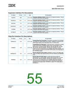
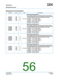
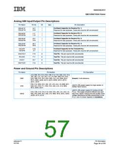
Serial DCC Interface Pin Descriptions (Sheet 2 of 2)
Pin Name
Pin No.
I/O
Type
Pin Description
DCC Receive Data 3:
Bit-serial D1-D3 or D4-D12 data from macro 3 of the SONET/SDH framer to
an external LAPD controller device. The data on this pin is output with the
R1DCLK3 clock.
R1DATA3
AC13
O
LVTTL-5sd
DCC Receive Data 4:
Bit-serial D1-D3 or D4-D12 data from macro 4 of the SONET/SDH framer to
an external LAPD controller device. The data on this pin is output with the
R1DCLK4 clock.
R1DATA4
R1DCLK1
R1DCLK2
R1DCLK3
R1DCLK4
AC15
AE07
AE09
AE13
AE15
O
O
O
O
O
LVTTL-5sd
LVTTL-5sd
LVTTL-5sd
LVTTL-5sd
LVTTL-5sd
DCC Receive Clock 1:
A bit clock from the SONET/SDH framer for clocking the data on the
R1DATA1 pin into an external LAPD controller or similar device. The clock
edge used for output of the R1DATA1 signal is selectable via a control bit.
DCC Receive Clock 2:
A bit clock from the SONET/SDH framer for clocking the data on the
R1DATA2 pin into an external LAPD controller or similar device. The clock
edge used for output of the R1DATA2 signal is selectable via a control bit.
DCC Receive Clock 3:
A bit clock from the SONET/SDH framer for clocking the data on the
R1DATA3 pin into an external LAPD controller or similar device. The clock
edge used for output of the R1DATA3 signal is selectable via a control bit.
DCC Receive Clock 4:
A bit clock from the SONET/SDH framer for clocking the data on the
R1DATA4 pin into an external LAPD controller or similar device. The clock
edge used for output of the R1DATA4 signal is selectable via a control bit.
ssframer.01
8/27/99
Pin Information
Page 45 of 279

 IBM [ IBM ]