IBM3009K2672
IBM SONET/SDH Framer
Input, Output and Input/Output Parameters
On-chip pull-up and pull-down resistors are in the range of 10 to 15 kΩ. This implies that pulling the pin volt-
age up or down requires hundreds of nanoseconds when an output driver switches to tri-state. Transitions will
be slower with large capacitive loads. For outputs going tri-state, where a slow transition might cause func-
tional problems, an external 1 to 3 kΩ pull-up or pull-down resistor should be used.
When connecting any LVTTL pin that does not have an internal pull resistor to another LVTTL pin that has an
internal pull-down resistor, an external pull-down resistor of 1-3 kΩ should be added to ensure that the signal
is pulled to the appropriate logic level when the driving signal goes tri-state. This only applies to connections
that have signals that go tri-state and we want to ensure that a valid logic level is present on the signals. An
example of this would be when two SONET/SDH framers are connected back-to-back across their Telecom
Bus interfaces. The signals that would need an external pull-down resistor are the TXTB#SPE to RXTB#SPE
connections and the TXTB#C1J1 to RXTB#C1J1 connections.
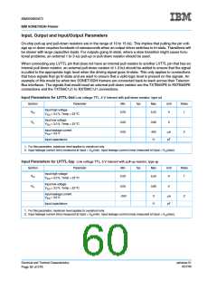
Input Parameters for LVTTL-5sd Low voltage TTL, 5 V tolerant with pull-down resistor, type sd
Symbol
Parameter
Min
Typ
Max
Unit
V
Notes
1
Input high voltage
VIH
2.00
5.50
V
DD = 3.0 V, Temp = 23 ο
C
Input low voltage
VIL
0.00
0.00
0.80
V
V
DD = 3.0 V, Temp = 23 ο
C
Input leakage current
VDD = 3.6 V
400
11
µA
2
Input capacitance
pF
1. For this parameter, maximum level applies to overshoot only.
2. Input leakage current (min) measured at Input = VIH(min). Input leakage current (max) measured at Input = VIH(max).
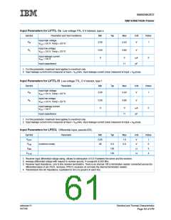
Input Parameters for LVTTL-5sp Low voltage TTL, 5 V tolerant with pull-up resistor, type sp
Symbol
Parameter
Min
Typ
Max
Unit
V
Notes
1
Input high voltage
VIH
2.00
5.50
V
DD = 3.0 V, Temp = 23 ο
C
Input low voltage
V
VIL
0.00
-250
0.80
V
DD = 3.0 V, Temp = 23 ο
C
Input leakage current
VDD = 3.6 V
0
µA
2
Input capacitance
11
pF
1. For this parameter, maximum level applies to overshoot only.
2. Input leakage current (min) measured at Input = VIH(min). Input leakage current (max) measured at Input = VIH(max).
Electrical and Thermal Characteristics
Page 52 of 279
ssframer.01
8/27/99

 IBM [ IBM ]