IBM3009K2672
IBM SONET/SDH Framer
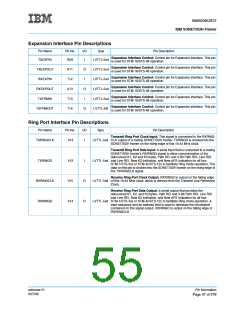
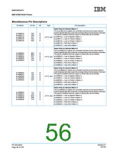
Serial DCC Interface Pin Descriptions (Sheet 1 of 2)
Pin Name
Pin No.
I/O
Type
Pin Description
DCC Transmit Data 1:
Bit-serial data from LAPD interface controller or similar device to
SONET/SDH macro 1 in the SONET/SDH framer. This data can optionally
be provided to either the D1-D3 or D4-D12 bytes in STM-1 #1/STS-3c #1 as
selected by a control bit. The data on this pin is sampled with the T1DCLK1
clock.
T1DATA1
AC19
I
LVTTL-5sd
DCC Transmit Data 2:
Bit-serial data from LAPD interface controller or similar device to
SONET/SDH macro 2 in the SONET/SDH framer. This data can optionally
be provided to either the D1-D3 or D4-D12 bytes in STM-1 #2/STS-3c #2 as
selected by a control bit. The data on this pin is sampled with the T1DCLK2
clock.
T1DATA2
T1DATA3
T1DATA4
AB19
AA19
Y19
I
I
I
LVTTL-5sd
LVTTL-5sd
LVTTL-5sd
DCC Transmit Data 3:
Bit-serial data from LAPD interface controller or similar device to
SONET/SDH macro 3 in the SONET/SDH framer. This data can optionally
be provided to either the D1-D3 or D4-D12 bytes in STM-1 #3/STS-3c #3 as
selected by a control bit. The data on this pin is sampled with the T1DCLK3
clock.
DCC Transmit Data 4:
Bit-serial data from LAPD interface controller or similar device to
SONET/SDH macro 4 in the SONET/SDH framer. This data can optionally
be provided to either the D1-D3 or D4-D12 bytes in STM-1 #4/STS-3c #4 as
selected by a control bit. The data on this pin is sampled with the T1DCLK4
clock.
DCC Transmit Clock 1:
The signals on T1DATA1 are sampled with this clock. This is a bit clock for
clocking either the D1-D3 or the D4-D12 DCC data bytes out of an external
LAPD controller or similar device into macro 1 of the SONET/SDH framer.
The clock edge used for data sampling is selectable via a control bit.
T1DCLK1
T1DCLK2
T1DCLK3
T1DCLK4
AA07
AA09
AA11
AA13
O
O
O
O
LVTTL-5sd
LVTTL-5sd
LVTTL-5sd
LVTTL-5sd
DCC Transmit Clock 2:
The signals on T1DATA2 are sampled with this clock. This is a bit clock for
clocking either the D1-D3 or the D4-D12 DCC data bytes out of an external
LAPD controller or similar device into macro 2 of the SONET/SDH framer.
The clock edge used for data sampling is selectable via a control bit.
DCC Transmit Clock 3:
The signals on T1DATA3 are sampled with this clock. This is a bit clock for
clocking either the D1-D3 or the D4-D12 DCC data bytes out of an external
LAPD controller or similar device into macro 3 of the SONET/SDH framer.
The clock edge used for data sampling is selectable via a control bit.
DCC Transmit Clock 4:
The signals on T1DATA4 are sampled with this clock. This is a bit clock for
clocking either the D1-D3 or the D4-D12 DCC data bytes out of an external
LAPD controller or similar device into macro 4 of the SONET/SDH framer.
The clock edge used for data sampling is selectable via a control bit.
DCC Receive Data 1:
Bit-serial D1-D3 or D4-D12 data from macro 1 of the SONET/SDH framer to
an external LAPD controller device. The data on this pin is output with the
R1DCLK1 clock.
R1DATA1
R1DATA2
AC09
AC11
O
O
LVTTL-5sd
LVTTL-5sd
DCC Receive Data 2:
Bit-serial D1-D3 or D4-D12 data from macro 2 of the SONET/SDH framer to
an external LAPD controller device. The data on this pin is output with the
R1DCLK2 clock.
Pin Information
ssframer.01
8/27/99
Page 44 of 279

 IBM [ IBM ]