IBM PowerPC 403GCX
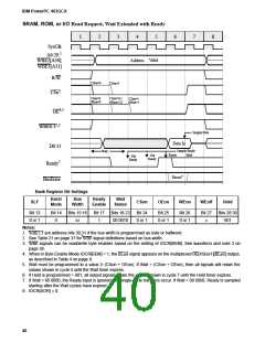
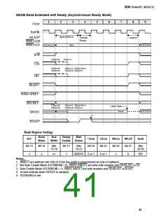
SRAM Read Extended with Ready (Asynchronous Ready Mode)
1
2
3
4
5
6
7
8
9
Cycle
SysClk
A6:A291
WBE2/A30
WBE3/A31
Sample
Ready
Wait=000010
Hold=01
Valid
R/W
CSx
CSon=0
CSon=1
CSon=0
OEon=0
CSon=1, OEon=0 or
CSon=0, OEon=1
OE2
BLAST3
WBE0:WBE32
BE0:BE33
D0:D31
CSon=0
OEon=0
CSon=1, OEon=0 or
CSon=0, OEon=1
Latch Data
Data In
4
READY
Bank Register Settings
Burst
Mode
Bus
Width
Ready
Enable
Wait
States
SLF
CSon
OEon
WEon
WEoff
Hold
Bit 13
Bit 14
Bits
15:16
Bit 17
Bits
18:23
Bit 24
Bit 25
Bit 26
Bit 27
0
Bits
28:30
x
o
xx
1
000010
0 or 1
0 or 1
x
001
Notes:
1. WBE2:3 are address bits A30:31 if the bus width is programmed as byte or halfword.
2. Not Byte Enable Mode (IOCR[BEM] = 0). WBE0:3/BE0:3 are write byte enables and OE/BLAST is OE.
3. Byte Enable Mode (IOCR[BEM] = 1). WBE0:3/BE0:3 are byte enables and OE/BLAST is BLAST
4. Arrows indicate when READY is sampled.
5. IOCR[ARE] is set.
41

 IBM [ IBM ]