IBM PowerPC 403GCX
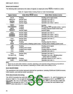
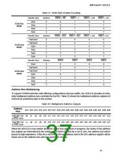
Table 21. Write Byte Enable Encoding
Transfer Size
Address
WBE0 = WE
WBE1 = 1
WBE2 = A30
WBE3 = A31
Byte
Byte
Byte
Byte
0
1
2
3
0
0
0
0
1
1
1
1
0
0
1
1
0
1
0
1
8-Bit Bus
Width
Transfer Size
Address
WBE0 = BHE
WBE1 = BLE
WBE2 = A30
WBE3 =A31
Half-word
Half-word
Byte
0
2
0
1
2
3
0
0
0
1
0
1
0
0
1
0
1
0
0
1
0
0
1
1
0
0
0
1
0
1
16-Bit Bus
Width
Byte
Byte
Byte
Transfer Size
Address
WBE0
WBE1
WBE2
WBE3
Word
Half-word
Half-word
Byte
0
0
2
0
1
2
3
0
0
1
0
1
1
1
0
0
1
1
0
1
1
0
1
0
1
1
0
1
0
1
0
1
1
1
0
32-Bit Bus
Width
Byte
Byte
Byte
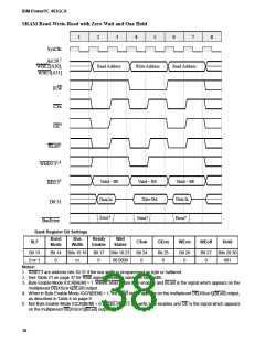
Address Bus Multiplexing
To support DRAM memories with differing configurations and bus widths, the 403GCX provides an inter-
nally multiplexed address bus controlled by the BIU. Table 22 shows the multiplexed address outputs ref-
erenced by waveforms later in this section.
Table 22. Multiplexed Address Outputs
Address
A11 A12 A13 A14 A15 A16 A17 A18 A19 A20 A21 A22 A23 A24 A25 A26 A27 A28 A29
Pins
Addr Bits Out a6 a7 a8 a9 a10 a11 a12 a13 a12 a13 a14 a15 a16 a17 a18 a19 a20 a21 a22
in RAS Cycle
Addr Bits Out xx a6 a7 a8 a9 a10 a11 a12 a21 a22 a23 a24 a25 a26 a27 a28 a29 a30 a31
in CAS Cycle
When the 403GCX is bus master and there are no bus operations in progress, the states of the address
bus outputs are determined by the setting of IOCR[ATC]. If this bit is set to zero, the address bus will be
placed in high impedance. If this bit is set to one, the last address held in the BIU address register will be
driven out on the address bus until bus operations resume.
37

 IBM [ IBM ]