IBM PowerPC 403GCX
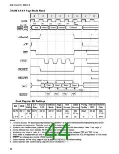
DRAM 2-1-1-1 Page Mode Read
1
2
3
4
5
6
7
8
SysClk
Pre-
Charge
RAS
CAS
CAS
CAS
CAS
A11:29,
WBE2[A30],
WBE3[A31]
Column4
Row Column1
Column2 Column3
AMuxCAS
R/W
RAS
CAS0:3
DRAMOE
DRAMWE
D0:31
Note 8
Data1
Data2
Data3
Data4
Note 7
Error
?
Error
?
Error
?
Error
?
BusError
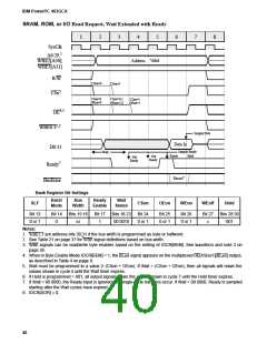
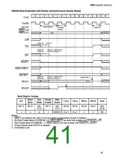
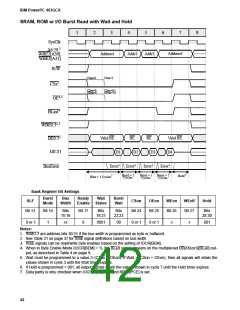
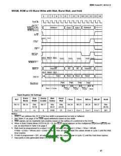
Bank Register Bit Settings
Bus
Width Mux
Ext RAS-to- Refresh Page
First
Burst
Prechg Refresh Refresh
SLF ERM
CAS
Mode
Mode Access Access Cycles
RAS
Rate
Bit 13 Bit 14 Bits Bit 17 Bit 18
15:16
Bit 19
Bit 20
Bits
21:22
Bits
23:24
Bit 25
Bit 26
Bits
27:30
0 or 1
0
xx
x
0
0
1
00
00
0
x
xxxx
Notes:
1. For burst access, the addresses represented by Columns 1 to 4 does not necessarily indicate that they are in
incremental address order. Typically, burst access is target word first.
2. If internal mux mode is used, address bits A11:29 represent address bits described in Table 22 on page 37.
3. During internal mux mode access, A6:10 retain their unmultiplexed values.
4. If external mux mode is used, A11:29 are unaffected and do not change between CAS and RAS cycles.
5. If bus width is programmed as byte or half-word, WBE2:3 represent address bits A30:31 regardless of mux mode.
6. WBE0:1 are always ones during DRAM transfers.
7. Data is latched on the rising edge of SysClk when IOCR[DRC] = 0 (default setting).
8. Data is latched later (on the rising edge of CAS) if IOCR[DRC] = 1.
44

 IBM [ IBM ]