IBM PowerPC 403GCX
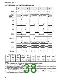
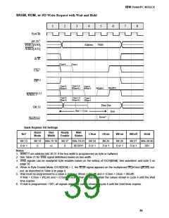
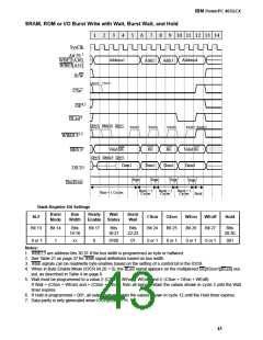
SRAM, ROM, or I/O Write Request with Wait and Hold
1
2
3
4
5
6
7
8
SysClk
A6:29,1
WBE2[A30],
Valid
Address
WBE3[A31]
R/W
CSon=0
CSon=1
CSx5
OE4,5
CSon=0
WEon=0
CSon=1,0
WEon=0,1
CSon=1
WEon=1
WEoff=0
WEoff=1
WBE0:32,3,5
CSon=0
OEon=0
CSon=1,0
OEon=0,1
CSon=1
OEon=1
Data Out
D0:31
Wait + 1 Cycle
Hold
Error?
BusError
Bank Register Bit Settings
Burst
Mode
Bus
Width
Ready
Enable
Wait
States
SLF
CSon
OEon
WEon
WEoff
Hold
Bit 13
0 or 1
Bit 14
0
Bits 15:16
xx
Bit 17
0
Bits 18:23
00 0011
Bit 24
0 or 1
Bit 25
0 or 1
Bit 26
0 or 1
Bit 27
0 or 1
Bits 28:30
001
Notes:
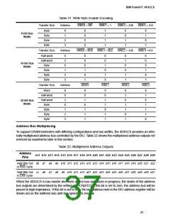
1. WBE2:3 are address bits 30:31 if the bus width is programmed as byte or halfword.
2. See Table 21 for WBE signal definitions based on bus width.
3. WBE signals can be read/write byte enables based on the setting of IOCR[BEM]. See waveform and note 3 on
page 38.
4. When in Byte Enable Mode IOCR[BEM] = 1, the BLast signal appears on the multiplexed OE[XSize1][BLast] out-
put, as described in Table 4 on page 9.
5. Wait must be programmed to a value ≥ (CSon + WEon + WEoff) and ≥ (CSon + OEon + WEoff).
If Wait > (CSon + WEon) and > (CSon + OEon), then all signals retain the values shown in cycle 4 until the Wait
time expires.
6. If Hold is programmed > 001, all signals retain the values shown in cycle 6 until the Hold timer expires.
39

 IBM [ IBM ]