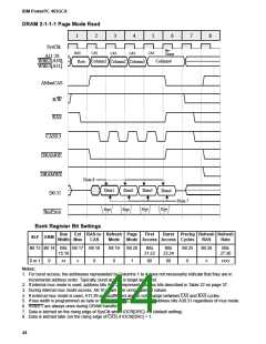
IBM PowerPC 403GCX
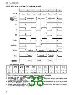
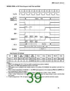
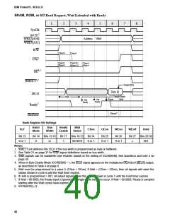
SRAM, ROM, or I/O Read Request, Wait Extended with Ready
1
2
3
4
5
6
7
8
SysClk
A6:29,1
WBE2[A30],
Address Valid
WBE3[A31]
R/W
CSon=0
CSon=1
CSx5
CSon=0
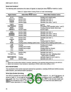
OEon=0
CSon=0,1
OEon=1,0
CSon=1
OEon=1
OE4,5
WBE0:32,3
Sample Data
Data In
D0:31
Sample Ready
Wait
Ready
Hold
Not
Ready
Not
Ready
Ready7
Error?
BusError
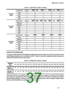
Bank Register Bit Settings
Burst
Mode
Bus
Width
Ready
Enable
Wait
States
SLF
CSon
OEon
WEon
WEoff
Hold
Bit 13
0 or 1
Bit 14
0
Bits 15:16
xx
Bit 17
1
Bits 18:23
00 0010
Bit 24
0 or 1
Bit 25
0 or 1
Bit 26
0 or 1
Bit 27
x
Bits 28:30
001
Notes:
1. WBE2:3 are address bits 30:31 if the bus width is programmed as byte or halfword.
2. See Table 21 on page 37 for WBE signal definitions based on bus width.
3. WBE signals can be read/write byte enables based on the setting of IOCR[BEM]. See waveform and note 3 on
page 38.
4. When in Byte Enable Mode IOCR[BEM] = 1, the BLast signal appears on the multiplexed OE[XSize1][BLast] output,
as described in Table 4 on page 9.
5. Wait must be programmed to a value ≥ (CSon + OEon). If Wait > (CSon + OEon), then all signals will retain the
values shown in cycle 4 until the Wait timer expires.
6. If Hold is programmed > 001, all output signals retain the values shown in cycle 7 until the Hold timer expires.
7. If Wait = 00 0000, the Ready input is ignored and single-cycle transfers occur. If Wait > 00 0000, Ready is sampled
starting after the Wait cycles have expired.
8. IOCR[SOR] = 0.
40

 IBM [ IBM ]