IBM PowerPC 403GCX
Reset and HoldAck
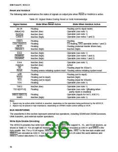
The following table summarizes the states of signals on output pins when Reset or HoldAck is active.
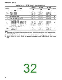
Table 20. Signal States During Reset or Hold Acknowledge
Signal Names
State When Reset Active
Floating
Inactive (low)
Inactive (low)
Inactive (high)
State When HoldAck Active
A6:29
AMuxCAS
BusReq
CAS0:3
Floating (set to input mode)
Operable (see note 1)
Operable (see note 1)
Operable (see notes 1 and 2)
CS0:3
CS4:7/RAS3:0
D0:31
Floating
Floating
Floating
Inactive (high)
Floating
CS floating, RAS operable (notes 1 and 2)
Floating (external master drives bus)
Inactive (high)
DMAA0:3
XAck
DRAMOE
DRAMWE
Inactive (high)
Inactive (high)
Inactive (high)
Operable (see note 1)
Operable (see notes 1 and 2)
Operable (see notes 1 and 2)
Error
HoldAck
OE
Inactive (low)
Inactive (low)
Floating
Operable (see note 1)
Active
Floating (input for XSize1)
Reset
Floating unless initiating system reset Floating unless initiating system reset
R/W
TC0:2
TC3
Floating
Floating (set to input)
Inactive (high)
Floating (input for XSize0)
Operable (see note 1)
Floating (set to input)
Floating (set to input)
Floating
TDO
TS0:2
TS3:6[DP3:0]
Inactive (low)
Floating
Operable (see note 1)
Operable (see note 1)[floating when
parity mode is enabled]
Floating
Inactive (high)
Operable (inputs for A4:5, A30:31)
Operable (see note 1)
WBE0:3[BE0:3]
XmitD
Note:
1. Signal may be active while HoldAck is asserted, depending on the operation being performed by the 403GCX.
2. Signal may be placed in high impedance, depending on DRAM 3-state control setting in IOCR.
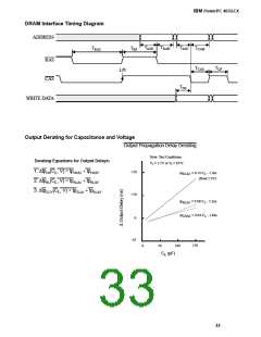
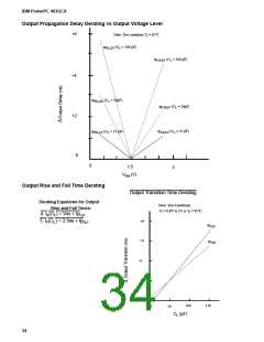
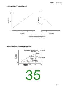
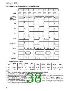
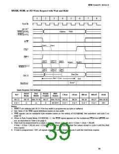
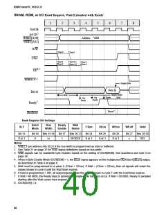
BUS WAVEFORMS
The waveforms in this section represent external bus operations, including SRAM and DRAM accesses,
DMA transfers, and external master operations.
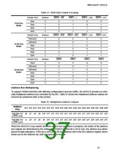
Write Byte Enable Encoding
The 403GCX provides four write byte enable signals (WBE0:3) to support 8-, 16-, and 32-bit devices, as
shown in Table 21. For an eight-bit memory region, WBE2:3 are encoded as A30:31 and WBE0 is the
byte-enable line. For a 16-bit region, WBE0 is the high-byte enable, WBE1 is the low-byte enable and
WBE2:3 are encoded as A30:31. For a 32-bit region, address bits 6:29 select the word address and
WBE0:3 select data bytes 0:3, respectively.
36

 IBM [ IBM ]