APCPCWM_4828539:WP_0000001WP_0000001
1
H27(U_S)4G8_6F2D
4 Gbit (512M x 8 bit) NAND Flash
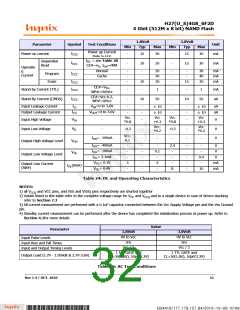
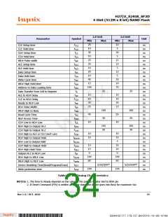
Item
Symbol
Test Condition
Min
Max
10
Unit
pF
CI/O
VIL= 0V
Input / Output Capacitance (1)
Input Capacitance (1)
-
-
CIN
VIN= 0V
10
pF
Table 26: Pin Capacitance (TA = 25C, f=1.0MHz)
NOTE: For the stacked devices version the Input Capacitance is 10pF x (number of stacked chips) and the I/O ca
pacitance is 10pF x (number of stacked chips)
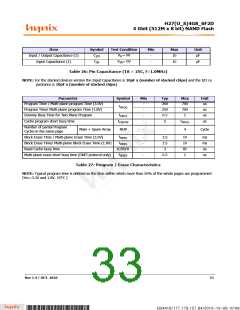
Parameter
Symbol
Min
Typ
200
250
0.5
Max
700
700
1
Unit
us
Program Time / Multi-plane program Time (3.0V)
Program Time/ Multi-plane program Time (1.8V)
Dummy Busy Time for Two Plane Program
-
-
-
tPROG
us
tDBSY
us
tCBSYW
tPROG
Cache program short busy time
-
-
5
-
us
Number of partial Program
Main + Spare Array
NOP
4
Cycle
Cycles in the same page
tBERS
tBERS
Block Erase Time / Multi-plane Erase Time (3.0V)
Block Erase Time/ Multi-plane Block Erase Time (1.8V)
Read Cache busy time
-
-
-
-
3.5
3.5
3
10
10
tR
1
ms
ms
us
tCBSYR
tIEBSY
Multi-plane erase short busy time (ONFI protocol only)
0.5
us
Table 27: Program / Erase Characteristics
NOTE: Typical program time is defined as the time within which more than 50% of the whole pages are programmed
(Vcc=3.3V and 1.8V, 25*C )
Rev 1.4 / OCT. 2010
33
B34416/177.179.157.84/2010-10-08 10:08
*ba53f20d-240c*

 HYNIX [ HYNIX SEMICONDUCTOR ]