APCPCWM_4828539:WP_0000001WP_0000001
1
H27(U_S)4G8_6F2D
4 Gbit (512M x 8 bit) NAND Flash
4. OTHER FEATURES
4.1 Data Protection and Power on / off sequence
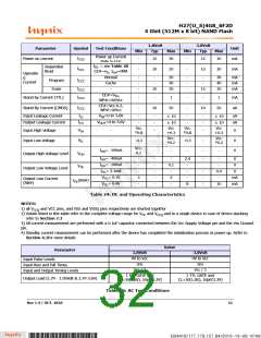
The device is designed to offer protection from any involuntary program/erase during power-transitions. An internal volt-
age detector disables all functions whenever Vcc is below about 1.8V (3V version), or 1.1V (1.8V version).
The power-up and power-down sequence is shown in Figure 32 in this case VCC and VCCQ on the one hand (and VSS
and VSSQ on the other hand) are shorted together at all times
The Ready/Busy signal shall be valid within 100us since the power supplies have reached the minimum values (as spec-
ified on), and shall return to one within 5msec (max).
During this busy time, the device executes the initialization process (cam reading), and dissipates a current ICC0 (30mA
max) in addition, it disregards all command excluding Read Status Register (70h).
At the end of this busy time, the device deaults into "read setup", thus if user decides to issue page read command, the
00h command may be skipped.
WP# pin provides hardware protection and is recommended to be kept at VIL during power-up and power-down. A re-
covery time of minimum 100usec is required before internal circuit gets ready for any command sequences as shown in
Figure 33. The two-step command sequence for program/erase provides additional software protection.
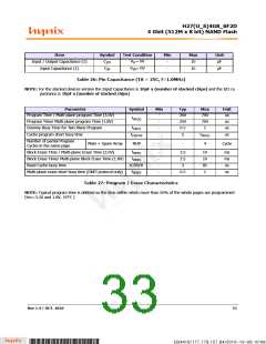
4.2 Ready/Busy.
The device has a Ready/Busy output that provides method of indicating the completion of a page program, erase, copy-
back, random read completion. The RB# pin is normally high and goes to low when the device is busy (after a reset,
read, program, erase operation). It returns to high when the internal controller has finished the operation. The pin is an
open-drain driver thereby allowing two or more RB# outputs to be Or-tied. Because pull-up resistor value is related to
tr(RB#) and current drain during busy (Ibusy), an appropriate value can be obtained with the following reference chart
(refer to Figure 34). Its value can be determined by the following guidance.
4.3 Write protect (#WP) handling
Erase and program operations are aborted if WP# is driven low during busy time, and kept low for about 100nsec.
Switching WP# low during this time is equivalent to issuing a Reset command (FFh)
The contents of memory cells being altered are no longer valid, as the data will be partially programmed or erased.
The R/B# pin will stay low for tRST (similarly to Figure 29). At the end of this time, the command register is ready to
process the next command, and the Status Register bit IO<6> will be cleared to "1", while IO<7> value will be related
to the WP# value.
Refer to Table 12 for more information on device status.
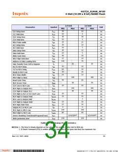
Erase and program operations are enabled or disabled by setting WP# to high or low respectively prior to issuing the set-
up commands (80h or 60h).
The level of WP# shall be set tWW nsec prior to raising the WE# pin for the set up command, as explained in Figure 35
and Figure 36.
Rev 1.4 / OCT. 2010
30
B34416/177.179.157.84/2010-10-08 10:08
*ba53f20d-240c*

 HYNIX [ HYNIX SEMICONDUCTOR ]