APCPCWM_4828539:WP_0000001WP_0000001
1
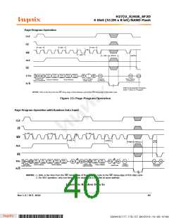
H27(U_S)4G8_6F2D
4 Gbit (512M x 8 bit) NAND Flash
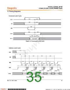
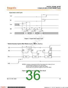
Input Data Latch Cycle
tCLH
CLE
tCH
CE
tWC
tALS
ALE
tWP
tWP
tWP
WE
tWH
tDH
tWH
tDH
tDH
tDS
tDS
tDS
I/Ox
DIN 0
DIN 1
DIN final
Figure 7: Input Data Latch Cycle
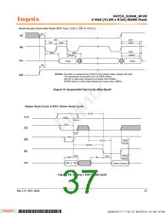
* Serial Access Cycle after Read (CLE=L, WE=H, ALE=L)
tRC
CE
tCHZ
tCOH
tREH
tREA
tREA
tREA
RE
tRHZ
tRHZ
tRHOH
I/Ox
Dout
Dout
Dout
tRR
R/B
NOTES: Transition is measured at ±±22mꢀ ꢁrom steadꢂ state ꢃoꢄtaꢅe ꢆitꢇ ꢄoadꢈ
Tꢇis parameter is sampꢄed and not 122% testedꢈ
tRLOH is ꢃaꢄid ꢆꢇen ꢁrequencꢂ is ꢇiꢅꢇer tꢇan 33MHzꢈ
tRHOH starts to be ꢃaꢄid ꢆꢇen ꢁrequencꢂ is ꢄoꢆer tꢇan 33MHzꢈ
Figure 8: Sequential Out Cycle after Read
Rev 1.4 / OCT. 2010
36
B34416/177.179.157.84/2010-10-08 10:08
*ba53f20d-240c*

 HYNIX [ HYNIX SEMICONDUCTOR ]