APCPCWM_4828539:WP_0000001WP_0000001
1
H27(U_S)4G8_6F2D
4 Gbit (512M x 8 bit) NAND Flash
1.8Volt
Typ
3.0Volt
Typ
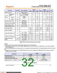
Parameter
Symbol
ICC0
Test Conditions
Unit
mA
Min
Max
Min
Max
Power up Current
Power on current
-
15
10
30
-
15
15
30
(Refer to 4.41)
tRC = see Table 28
CE#=vIL, Iout=0MA
Sequential
Read
ICC1
-
20
-
30
mA
Operatin
g
Current
Normal
Cache
-
-
-
-
-
-
20
30
20
-
-
-
-
-
30
40
30
mA
mA
mA
ICC2
ICC3
ICC4
Program
Erase
10
15
CE#=VIH,
WP#=0V/Vcc
Stand-by Current (TTL)
-
-
-
1
-
-
-
1
mA
uA
CE#=Vcc-0.2,
WP#=0/Vcc
ICC5
Stand-By Current (CMOS)
10
50
10
50
ILI
VIN=0 to 3.6V
Input Leakage Current
Output Leakage Current
-
-
-
-
-
-
-
-
uA
uA
± 10
± 10
± 10
± 10
ILO
VOUT=0 to 3.6V
Vcc
*0.8
Vcc
+0.3
Vcc
*0.8
Vcc
+0.3
VIH
VIL
Input High Voltage
Input Low Voltage
-
-
-
-
-
-
V
V
V
Vcc-
*0.2
Vcc
*0.2
-
-0.3
-0.3
-
Vcc-
0.1
IOH= -100uA
-
-
-
VOH
Output High Voltage Level
Output Low Voltage Level
I
OH= -400uA
-
-
-
-
-
-
-
-
0.1
-
2.4
--
-
-
V
V
IOH= -100uA
IOL= 2.1mA
VOL= 0.1V
VOL= 0.4V
-
-
VOL
-
-
-
-
0.4
-
V
3
-
4
-
mA
mA
Output Low Current
(RB#)
IOL(RB#)
-
8
10
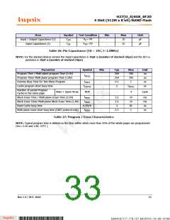
Table 24: DC and Operating Characteristics
NOTES:
1) all VCCQ and VCC pins, and VSS and VSSQ pins respectively are shorted together
2) Values listed in this table refer to the complete voltage range for VCC and VCCQ and to a single device in case of device stacking
refer to Section 7.3
3) All current measurement are performed with a 0.1uF capacitor connected between the Vcc Supply Voltage pin and the Vss Ground
pin.
4) Standby current measurement can be performed after the device has completed the initialization process at power up. Refer to
Section 4.1for more details
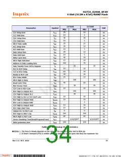
Value
Parameter
1.8Volt
0V to Vcc
5ns
3.0Volt
0V to Vcc
5ns
Input Pulse Levels
Input Rise and Fall Times
Input and Output Timing Levels
Vcc / 2
Vcc / 2
1 TTL GATE and
CL=30(1.8V), 50pF(3.3V)
1 TTL GATE and
CL=30(1.8V), 50pF(3.3V)
Output Load (1.7V - 1.95Volt & 2.7V-3.6V)
Table 25: AC Test Conditions
Rev 1.4 / OCT. 2010
32
B34416/177.179.157.84/2010-10-08 10:08
*ba53f20d-240c*

 HYNIX [ HYNIX SEMICONDUCTOR ]