APCPCWM_4828539:WP_0000001WP_0000001
1
H27(U_S)4G8_6F2D
4 Gbit (512M x 8 bit) NAND Flash
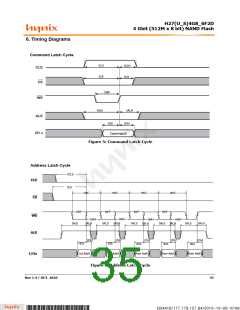
6. Timing Diagrams
Command Latch Cycle
tCL
S
tCLH
tCH
CLE
tCS
CE
tWP
WE
tALS
tALH
ALE
I/O x
tDS
tDH
Command
Figure 5: Command Latch Cycle
Address Latch Cycle
W&/6
&/(
W&6
W:&
W:&
W:&
W:&
&(
W:3
W:3
W:3
W:3
:(
W:+
W$/+
W:+
W$/+
W:+
W$/+
W:+
W$/+
W$/6
W$/6
W$/6
W$/6
W$/6
W$/+
W'+
$/(
W'+
W'+
W'+
W'+
W'6
W'6
W'6
W'6
W'6
&ROꢀ$GGꢁ
&ROꢀ$GGꢂ
5RZꢃ$GGꢁ
5RZꢃ$GGꢂ
5RZꢃ$GGꢄ
,ꢀ2[
Figure 6: Address Latch Cycle
Rev 1.4 / OCT. 2010
35
B34416/177.179.157.84/2010-10-08 10:08
*ba53f20d-240c*

 HYNIX [ HYNIX SEMICONDUCTOR ]