APCPCWM_4828539:WP_0000001WP_0000001
1
H27(U_S)4G8_6F2D
4 Gbit (512M x 8 bit) NAND Flash
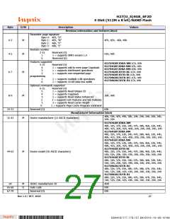
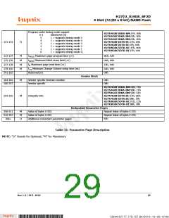
Program cache timing mode support
H27U4G8F2DKA-BM:1Fh, 00h
H27S4G8F2DKA-BM:03h, 00h
H27S4G6F2DKA-BM:03h, 00h
H27U4G8F2DTR-BC:1Fh, 00h
H27U4G8F2DTR-BI:1Fh, 00h
H27U8G8G5DTR-BC:1Fh, 00h
H27U8G8G5DTR-BI:1Fh, 00h
6-1
5Reserved (0)
5
4
3
2
1
0
1 = supports timing mode 5
1 = supports timing mode 4
1 = supports timing mode 3
1 = supports timing mode 2
1 = supports timing mode 1
1 = supports timing mode 0,
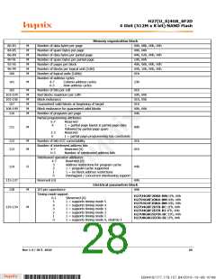
131-132
O
tPROG Maximum page program time (㎲)
tBERS Maximum block erase time (㎲)
tR Maximum page read time (㎲)
tccs Minimum Change Column setup time (ns)
Reserved (0)
133-134
135-136
137-138
M
M
M
M
BCh, 02h
0Ah, 00h
19h, 00h
139-140
141-163
64h, 00h
00h
Vendor block
164-165
166-253
M
M
Vendor specific Revision number
Vendor specific
00h
00h
H27U4G8F2DKA-BM:48h, F6h
H27S4G8F2DKA-BM:9Bh, CEh
H27S4G6F2DKA-BM:54h, 61h
H27U4G8F2DTR-BC:1Fh, EDh
H27U4G8F2DTR-BI:5Bh, 14h
H27U8G8G5DTR-BC:FCh, C1h
H27U8G8G5DTR-BI:B8h, 38h
254-255
Integrita CRC
Redundant Parameter Pages
256-511
512-767
768+
M
M
O
Value of bytes 0-255
Repeat Value of bytes 0-255
Repeat Value of bytes 0-255
FFh
Value of bytes 0-255
Additional redundant parameter pages
Table 21: Parameter Page Description
NOTE: “O” Stands for Optional, “M” for Mandatory
Rev 1.4 / OCT. 2010
29
B34416/177.179.157.84/2010-10-08 10:08
*ba53f20d-240c*

 HYNIX [ HYNIX SEMICONDUCTOR ]