APCPCWM_4828539:WP_0000001WP_0000001
1
H27(U_S)4G8_6F2D
4 Gbit (512M x 8 bit) NAND Flash
1.8 Volt
Max
3.0 Volt
Max
Parameter
Symbol
Unit
Min
25
10
35
10
25
25
10
20
10
45
15
100
Min
12
5
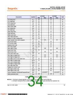
tCLS
tCLH
tCS
CLE Setup time
CLE Hold time
CE# Setup time
CE# Hold time
ns
ns
ns
ns
ns
ns
ns
ns
ns
ns
ns
ns
us
ns
ns
ns
ns
ns
ns
ns
ns
ns
ns
ns
ns
ns
ns
ns
ns
ns
ns
ns
ns
20
5
tCH
12
12
5
tWP
tALS
tALH
tDS
WE# Pulse width
ALE Setup time
ALE Hold time
12
5
Data Setup time
tDH
Data Hold time
25
10
70
tWC
tWH
tADL
tR
Write Cycle time
WE# High Hold time
Address to Data Loading time
Data Transfer from Cell to Register
ALE to RE# Delay
25
25
10
10
20
25
10
10
20
12
tAR
tCLR
tRR
CLE to RE# Delay
Ready to RE# Low
tRP
RE# Pulse Width
100
30
100
20
tWB
tRC
tREA
tCR
WE# High to Busy
45
10
25
10
Read Cycle Time
RE# Access Time
CE# Low to RE# Low
RE# High to Output Hi-Z
CE# High to Output Hi-Z
CE# High to ALE or CLE Don't care
RE# High to Output Hold
RE# Low to Output Hold
CE# High to Output Hold
RE# High Hold Time
Output Hi-Z to RE# Low
RE# High to WE# Low
WE# High to RE# Low
Device Resetting Time(Read/Program/Erase)
Write protection time
100
30
100
30
tRHZ
tCHZ
tCSD
tRHOH
tRLOH
tCOH
tREH
tIR
10
15
-
10
15
5
15
15
0
15
10
0
100
60
-
100
60
tRHW
tWHR
tRST
tWW
5/10/500(2)
5/10/500(2)
100
100
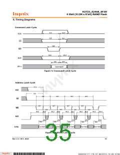
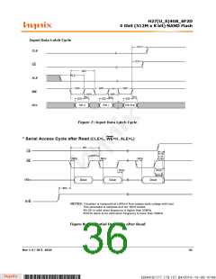
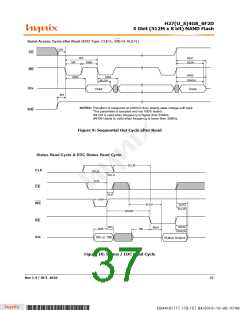
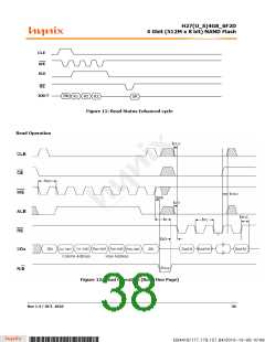
Table 28: AC Timing Characteristics
NOTES: 1. The time to Ready depends on the value of the pull-up resistor tied to RB# pin
2. If Reset Command (FFh) is written at Ready state, the device goes into Busy for maximum 5us
Rev 1.4 / OCT. 2010
34
B34416/177.179.157.84/2010-10-08 10:08
*ba53f20d-240c*

 HYNIX [ HYNIX SEMICONDUCTOR ]