APCPCWM_4828539:WP_0000001WP_0000001
1
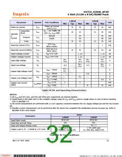
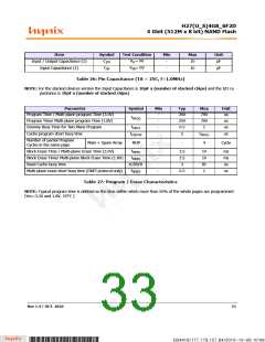
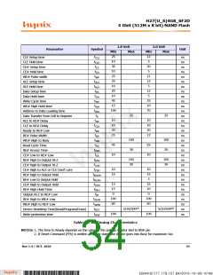
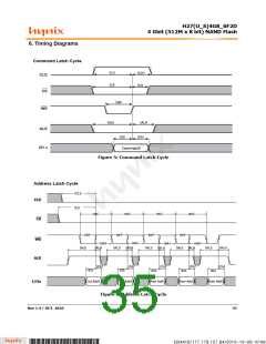
H27(U_S)4G8_6F2D
4 Gbit (512M x 8 bit) NAND Flash
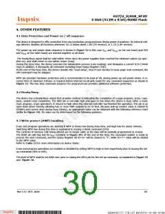
WE
IO[7:0]
VALID
WP
SEQUENCE
ABORTED
> 100nsec
Figure 5: WP# low timing requirements during program/erase command sequence
5. Device Parameters
Parameter
Symbol
Min
4016
Typ
Max
4096
8192
16284
Unit
Blocks
Blocks
Blocks
NVB
Valid Block Numbe, 4Gb
Valid Block Numbe, 8Gb
Valid Block Numbe, 16Gb
-
-
-
NVB
NVB
8032(*)
16064(*)
Table 22: Valid Blocks Number
(*) Each 4Gb has maximum 80 bad blocks
NOTE: The 1st block is quranteed to be a valid blick at the time of shipment.
Value
3.0
Symbol
Parameter
Unit
Ambient Operating Temperature (Temperature Range Option 1)
Ambient Operating Temperature (Temperature Range Option 6)
Temperature Under Bias
0 to 70
-40 to 85
-50 to 125
°C
°C
°C
TA
TBIAS
TSTG
Storage Temperature
Input or Output Voltage
Supply Voltage
-60 to 150
-0.6 to 4.6
-0.6 to 4.6
°C
V
(2)
VIO
VCC
V
Table 23: Absolute maximum ratings
NOTES:
1. Except for the rating "Operating Temperature Range", stresses above those listed in the Table "Absolute Maximum
Ratings" may cause permanent damage to the device. These are stress ratings only and operation of the device at
these or any other conditions above those indicated in the Operating sections of this specification is not implied. Expo
sure to Absolute Maximum Rating conditions for extended periods may affect device reliability. Refer also to the STMi
croelectronics SURE Program and other relevant quality documents.
2. Minimum Voltage may undershoot to -2V during transition and for less than 20ns during transitions.
Rev 1.4 / OCT. 2010
31
B34416/177.179.157.84/2010-10-08 10:08
*ba53f20d-240c*

 HYNIX [ HYNIX SEMICONDUCTOR ]