APCPCWM_4828539:WP_0000001WP_0000001
1
H27(U_S)4G8_6F2D
4 Gbit (512M x 8 bit) NAND Flash
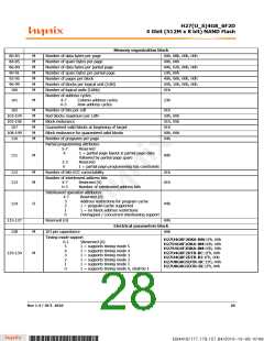
Memory organization block
80-83
84-85
86-89
90-91
92-95
96-99
100
M
M
M
M
M
M
M
Number of data bytes per page
Number of spare bytes per page
Number of data bytes per partial page
Number of spare bytes per partial page
Number of pages per block
00h, 08h, 00h, 00h
40h, 00h
00h, 02h, 00h, 00h
10h, 00h
40h, 00h, 00h, 00h
00h, 10h, 00h, 00h
01h
Number of blocks per logical unit (LUN)
Number of logical units (LUNs)
Number of address cycles
101
102
M
4-7
0-3
Column address cycles
Row address cycles
23h
M
M
M
M
M
M
Number of bits per cell
01h
103-104
105-106
107
Bad blocks maximum per LUN
Block endurance
50h, 00h
01h, 05h
01h
Guaranteed valid blocks at beginning of target
Block endurance for guaranteed valid blocks
Number of programs per page
Partial programming attributes
108-109
110
00h, 00h
04h
5-7
4
Reserved
1 = partial page layout is partial page data
followed by partial page spare
Reserved
111
M
00h
1-3
0
1 = partial page programming has constraints
112
113
M
M
Number of bits ECC correctability
Number of interleaved address bits
01h
01h
4-7
Reserved (0)
0-3
Number of interleaved address bits
Interleaved operation attributes
4-7
Reserved (0)
3
2
1
0
Address restrictions for program cache
1 = program cache supported
1 = no block address restrictions
Overlapped / concurrent interleaving support
114
O
04h
00h
115-127
128
Reserved (0)
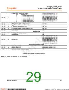
Electrical parameters block
0Ah
M
M
I/O pin capacitance
Timing mode support
H27U4G8F2DKA-BM:1Fh, 00h
H27S4G8F2DKA-BM:03h, 00h
H27S4G6F2DKA-BM:03h, 00h
H27U4G8F2DTR-BC:1Fh, 00h
H27U4G8F2DTR-BI:1Fh, 00h
H27U8G8G5DTR-BC:1Fh, 00h
H27U8G8G5DTR-BI:1Fh, 00h
6-1
5
4
3
2
1
0
5Reserved (0)
1 = supports timing mode 5
1 = supports timing mode 4
1 = supports timing mode 3
1 = supports timing mode 2
1 = supports timing mode 1
1 = supports timing mode 0, shall be 1
129-130
Rev 1.4 / OCT. 2010
28
B34416/177.179.157.84/2010-10-08 10:08
*ba53f20d-240c*

 HYNIX [ HYNIX SEMICONDUCTOR ]