HC6856
DYNAMIC ELECTRICAL CHARACTERISTICS
Write Cycle
Read Cycle
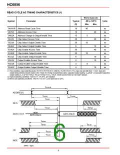
The RAM is asynchronous in operation, allowing the read
cycletobecontrolledbyaddress,chipselect(NCS),orchip
enable (CE) (refer to Read Cycle timing diagram). To
perform a valid read operation, both chip select and output
enable (NOE) must be low and chip enable and write
enable (NWE) must be high. The output drivers can be
controlled independently by the NOE signal. Consecutive
read cycles can be executed with NCS held continuously
low, and with CE held continuously high.
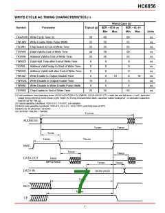
The write operation is synchronous with respect to the
address bits, and control is governed by write enable
(NWE), chip select (NCS), or chip enable (CE) edge
transitions (refer to Write Cycle timing diagrams). To per-
form a write operation, both NWE and NCS must be low,
and CE must be high. Consecutive write cycles can be
performed with NWE or NCS held continuously low, or CE
held continuously high. At least one of the control signals
must transition to the opposite state between consecutive
write operations.
For an address activated read cycle, NCS and CE must be
valid prior to or coincident with the activating address edge
transition(s). Any amount of toggling or skew between
address edge transitions is permissible; however, data
outputs will become valid TAVQV time following the latest
occurring address edge transition. The minimum address
activated read cycle time is TAVAV. When the RAM is
operated at the minimum address activated read cycle
time, the data outputs will remain valid on the RAM I/O until
TAXQX time following the next sequential address transi-
tion.
The write mode can be controlled via three different control
signals: NWE, NCS, and CE. All three modes of control are
similar except the NCS and CE controlled modes actually
disable the RAM during the write recovery pulse. Only the
NWE controlled mode is shown in the table and diagram on
the previous page for simplicity; however, each mode of
control provides the same write cycle timing characteris-
tics. Thus, someoftheparameternamesreferencedbelow
are not shown in the write cycle table or diagram, but
indicate which control pin is in control as it switches high or
low.
To control a read cycle with NCS, all addresses and CE
must be valid prior to or coincident with the enabling NCS
edge transition. Address or CE edge transitions can occur
later than the specified setup times to NCS; however, the
valid data access time will be delayed. Any address edge
transition, which occurs during the time when NCS is low,
will initiate a new read access, and data outputs will not
becomevaliduntilTAVQVtimefollowingtheaddressedge
transition. Data outputs will enter a high impedance state
TSHQZ time following a disabling NCS edge transition.
TowritedataintotheRAM,NWEandNCSmustbeheldlow
and CE must be held high for at least TWLWH/TSLSH/
TEHEL time. Any amount of edge skew between the
signals can be tolerated, and any one of the control signals
can initiate or terminate the write operation. For consecu-
tivewriteoperations, writepulsesmustbeseparatedbythe
minimumspecifiedTWHWL/TSHSL/TELEHtime.Address
inputs must be valid at least TAVWL/TAVSL/TAVEH time
before the enabling NWE/NCS/CE edge transition, and
must remain valid during the entire write time. A valid data
overlapofwritepulsewidthtimeofTDVWH/TDVSH/TDVEL,
and an address valid to end of write time of TAVWH/
TAVSH/TAVEL also must be provided for during the write
operation. Hold times for address inputs and data inputs
with respect to the disabling NWE/NCS/CE edge transition
must be a minimum of TWHAX/TSHAX/TELAX time and
TWHDX/TSHDX/TELDX time, respectively. The minimum
write cycle time is TAVAV.
To control a read cycle with CE, all addresses and NCS
must be valid prior to or coincident with the enabling CE
edge transition. Address or NCS edge transitions can
occur later than the specified setup times to CE; however,
the valid data access time will be delayed. Any address
edge transition which occurs during the time when CE is
high will initiate a new read access, and data outputs will
not become valid until TAVQV time following the address
edge transition. Data outputs will enter a high impedance
state TELQZ time following a disabling CE edge transition.
8

 HONEYWELL [ Honeywell ]