HC6856
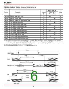
READ CYCLE AC TIMING CHARACTERISTICS (1)
Worst Case (3)
Symbol
Parameter
Typical
(2)
-55 to 125°C
Units
Min
Max
TAVAVR Address Read Cycle Time
18
18
15
20
20
6
40
ns
ns
ns
ns
ns
ns
ns
ns
ns
ns
ns
ns
TAVQV
TAXQX
TSLQV
TSLQX
TSHQZ
TEHQV
TEHQX
TELQZ
TGLQV
TGLQX
TGHQZ
Address Access Time
40
40
Address Change to Output Invalid Time
Chip Select Access Time
5
Chip Select Output Enable Time
Chip Select Output Disable Time
Chip Enable Access Time
16
10
40
20
20
6
Chip Enable Output Enable Time
Chip Enable Output Disable Time
Output Enable Access Time
16
0
10
10
4
Output Enable Output Enable Time
Output Enable Output Disable Time
3
4
10
(1) Test conditions: input switching levels VIL/VIH=0.5V/VDD-0.5V (CMOS), VIL/VIH=0V/3V (TTL), input rise and fall times <1 ns/V, input and
output timing reference levels shown in the Tester AC Timing Characteristics table, capacitive output loading CL >50 pF, or equivalent capacitive
output loading CL=5 pF for TSHQZ, TELQZ TGHQZ. For CL >50 pF, derate access times by 0.02 ns/pF (typical).
(2) Typical operating conditions: VDD=5.0 V, TA=25°C, pre-radiation.
(3) Worst case operating conditions: VDD=4.5 V to 5.5 V, post total dose at 25°C.
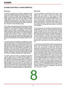
T
AVAVR
ADDRESS
NCS
T
AVQV
TAXQX
T
SLQV
T
SLQX
TSHQZ
HIGH
IMPEDANCE
DATA OUT
DATA VALID
T
EHQX
EHQV
T
TELQZ
CE
T
GLQX
GLQV
T
TGHQZ
NOE
(NWE = high)
6

 HONEYWELL [ Honeywell ]