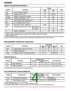
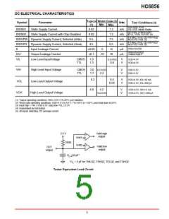
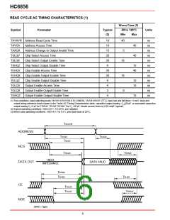
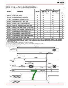
HC6856
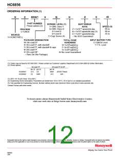
ORDERING INFORMATION (1)
40
H
Q
H
6856/1
X
Z
C
C
PART NUMBER
Pinout options (2)
SCREEN LEVEL (1)
V=QML Class V
Q=QML Class Q
S=Level S
B=Level B
E=Engr Device (4)
SOFT ERROR
RATE
SPEED (5)
60 ns
Z=<1x10⁻¹⁰ upsets/bit-day
PROCESS
C=CMOS
A=<1x10⁻⁹ upsets/bit-day (3)
C=<1x10⁻⁷ upsets/bit-day
- =No SER Guaranteed
40 ns
35 ns
SOURCE
H=HONEYWELL
PACKAGE DESIGNATION
W=36-Lead FP
X=36-Lead FP, with standoff
Y=36-Lead FP, with standoff & caps
N=28-Lead FP
TOTAL DOSE
HARDNESS
INPUT BUFFER TYPE
C=CMOS Level
T=TTL Level
R=1x10⁵rad(SiO2)
F=3x10⁵ rad(SiO2)
H=1x10⁶ rad(SiO2)
N=No Level Guaranteed
R=28-Lead DIP
- = Bare Die (No Package)
(1) Orders may be faxed to 612-954-2051. Please contact our Customer Logistics Department at 612-954-2888 for further information.
(2) Pinout options:
36-Lead FP
28-Lead FP & DIP
pin 32 pin 33
pin 34
HC6856/1
HC6856/2
A13
CE
CE
NWE
A13
JEDEC Pinout
N/A
NWE
(3) SER <1E-10 u/b-d from -55 to 80°C.
(4) Engineering Device description: Parameters are tested from -55 to 125°C, 24 hr burn-in, no radiation guaranteed.
(5) Only specified for Engineering Devices. Number defines worst case maximum Write Cycle time in nano-seconds (ns).
Contact Factory with other needs.
To lea r n m or e a bou t Hon eyw ell Solid Sta te Electr on ics Cen ter ,
visit ou r w eb site a t h ttp ://w w w .ssec.h on eyw ell.com
Honeywell reserves the right to make changes to any products or technology herein to improve reliability, function or design. Honeywell does not assume any liability
arising out of the application or use of any product or circuit described herein; neither does it convey any license under its patent rights nor the rights of others.
Helping You Control Your World
900049
2/96
12

 HONEYWELL [ Honeywell ]