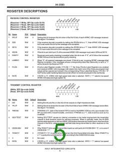
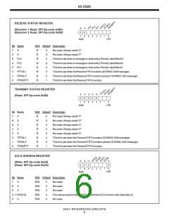
HI-3593
FUNCTIONAL DESCRIPTION
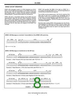
INITIALIZATION
ARINC 429 RECEIVERS
The HI-3593 has two completely independent ARINC 429 receive
channels. Each channel has an on-chip analog line receiver for
connection to the ARINC 429 incoming data bus. The ARINC 429
specification requires the following detection levels:
The HI-3593 may be initialized using the Master Reset (MR) pin or
under software control by executing SPI op-code 0x04. MR must
be pulsed high for 1 µs to bring the part to its completely reset
state. MR clears all three FIFOs, all six Priority-Label Mail Boxes,
clears the Filter memories and Match registers and sets all other
internal registers to their default state.
STATE
DIFFERENTIALVOLTAGE
ONE
NULL
ZERO
+6.5 Volts to +13 Volts
+2.5 Volts to -2.5 Volts
-6.5 Volts to -13 Volts
Software Reset is performed using SPI op-code 0x44. Software
Reset clears all three FIFOs and all six Priority-Label Mail Boxes,
but does not affect the values stored in the filter memories,
Priority-Label Match registers or other writeable registers. The
Transmit and Receive Status Registers will reflect the state of the
post-software reset device.
The HI-3593 guarantees recognition of these levels with a common
mode voltage with respect to GND less than 30V for the worst case
condition (3.15V supply and 13V signal level).
CLOCK FREQUENCY SELECTION
Design tolerances guarantee detection of the above levels, so the
actual acceptance ranges are slightly larger. If the ARINC signal
(including nulls) is outside the differential voltage ranges, the HI-
3593 receiver rejects the data.
For correct ARINC 429 data rate transmission and reception, and
bit timing, the HI-3593 transmit and receive logic requires a 1 MHz
+/- 1% reference clock source. The clock is input at the ACLK pin
and must be 1 MHz or any even multiple of 1 MHz up to 30 MHz. If
a clock source greater than 1 MHz is used, then the ACLK Division
Register must be programmed with the appropriate scaling value.
BIT TIMING
The ARINC 429 specification defines the following timing toler-
ances for received data:
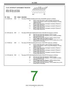
Note that the least significant bit of the ACLK Division Register is
fixed at “0” allowing only even numbers to be programmed.
Similarly the three most significant bits are also fixed at “0” limiting
the maximum value to 0x1E. The ACLK Division Register is
cleared to 0x00 after Master Reset and is unaffected by Software
Reset. When programmed to 0x00, the ACLK division ratio is one,
and a 1 MHz clock should be applied to ACLK. The ACLK Division
Register is loaded using SPI Op-Code 0x38 and read using Op-
Code 0xD4.
HIGH SPEED
LOW SPEED
(RATE = “0”)
(RATE = “1”)
BIT RATE
100K BPS 1%
1.5 0.5 µsec
1.5 0.5 µsec
5 µsec 5%
12K -14.5K BPS
10 5 µsec
10 5 µsec
PULSE RISE TIME
PULSE FALL TIME
PULSE WIDTH
34.5 to 41.7 µsec
The following table provides examples of ACLK frequency and
ACLK Division Register values for correct ARINC 429 operation:
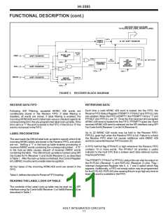
The HI-3593 accepts signals within these tolerances and rejects
signals outside these tolerances. Receiver logic achieves this as
described below:
ACLK Division Register value
External Clock
1. An accurate 1MHz clock source is required to validate the
receive signal timing.
0x00
0x02
0x04
0x06
0x08
0x0A
“
1 MHz
2 MHz
4 MHz
6 MHz
8 MHz
10 MHz
“
2. The receiver uses three separate 10-bit sampling shift reg-
isters for Ones detection, Zeros detection and Null detection.
When the input signal is within the differential voltage range
for any shift register’s state (One, Zero or Null) sampling
clocks a “1” into that register. When the receive signal is out-
side the differential voltage range defined for any shift regis-
ter, a “0” is clocked. Only one shift register can clock a “1” for
any given sample. All three registers clock zeros if the differ-
ential input voltage is between defined state voltage bands.
“
“
0x1C
0x1E
28 MHz
30 MHz
TABLE 2. ACLK DIVISION
Valid data bits require at least three consecutive One or Zero
samples (three “1’s”) in the first five positions of the Ones or
Zeros sampling shift register, and at least three consecutive
Null samples (three “1’s”) in the second five positions of the
Null sampling shift register within the data bit interval.
CONFIGURATION
The Transmit Control Register and Receiver Control Registers are
used to configure the ARINC 429 transmission channel and two
ARINC 429 receive channels. The registers may be written or read
at any time. They are reset to 0x00 following Master Reset and are
unchanged by Software Reset. Refer to the Receiver Control
Register and Transmit Control Register descriptions for detailed
information.
A word gap Null requires at least three consecutive Null sam-
ples in the first half of the Null sampling shift register and at
least three consecutive Null samples in the second half of the
Null sampling shift register. This guarantees the minimum
pulse width.
HOLT INTEGRATED CIRCUITS
9

 HOLTIC [ HOLT INTEGRATED CIRCUITS ]