HI-3593
FUNCTIONAL DESCRIPTION (cont.)
3. To validate the receive data bit rate, each bit must follow its All three Priority-Label Match Registers are loaded using SPI op-
preceding bit by not less than 8 samples and not more than 12 code 0x18 (Receiver 1) or 0x2C (Receiver 2), followed by three label
samples. With exactly 1MHz input clock frequency, the match values. The first byte is the match value for Priority-Label
acceptable data bit rates are:
Register #3, the second for Priority-Label Register #2 and the third
for Priority-Label #1. The match values may be checked by reading
the Priority-Label Match Registers using SPI op-code 0x9C
(Receiver 1) or 0xBC (Receiver 2).
HIGH SPEED LOW SPEED
DATA BIT RATE MIN
DATA BIT RATE MAX
83K BPS
125K BPS
10.4K BPS
15.6K BPS
When using the Priority-Label feature, all three Priority-Label Match
Registers must be loaded to avoid unintended matches occurring on
un-programmed Priority-Label Match Register random values. If
less than three Priority-Labels are required for a particular
application, duplicate copies of the same match value should be
stored in two (or three) registers.
4. Following the last data bit of a valid reception, the Word
Gap timer samples the Null shift register every 10 input
clocks (every 80 clocks for low speed). If a Null is present,
the Word Gap counter is incremented. A Word Gap count of
3 enables the next reception.
Note that Priority-Label Registers (mail boxes) are only 24 bits long.
Because the ARINC 429 label byte value is pre-programmed for
each register it is not necessary to store it when words are received.
This allows a shorter and faster access of the data field using SPI
Op-Codes 0xA4, 0xA8 and 0xAC (Receiver 1 Priority-Label
Registers #1, #2 and #3) or 0xC4, 0xC8 and 0xCC (Receiver 2
Priority-Label Registers #1, #2 and #3).
RECEIVER PARITY
Receiver parity checking is enabled by setting the Receive Control
register PARITY bit to a “1”. When enabled, the receiver parity
circuit counts Ones received, including the parity bit. If the result is
odd, a "0" is stored in the 32nd bit position, overwriting the received
parity bit. The “0” indicates a parity bit check pass.
The Receive Status Register bits PL1, PL2 and PL3 indicate when
Priority-Label data is available in the Priority-Label Registers. Six
status output pins MB1-1 through MB2-3 also indicate when data is
available at each of the six Priority-Label Registers. The R1INT and
R2INT interrupt pins can also be triggered when Priority Labels are
captured by programming bits 7, 6, 3 and 2 of the Flag / Interrupt
Assignment Register.
If receive parity is enabled and a word is received with bad odd
parity, the 32nd bit is overwritten with a “1” indicating a parity check
fail.
When the Receiver Control Register PARITY bit is a “0”, no parity
checking takes place and all 32 bits of the received word remain
unaltered.
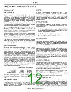
LABREC ARINC word
matches
Enabled
SDON
ARINC word
bits 10, 9
match
FIFO
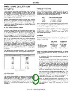
RECEIVED DATA ACCEPTANCE AND STORAGE
label
SD10, SD9
The HI-3593 subjects incoming ARINC 429 messages to three
different data filter checks before data is accepted. First all words are
filtered for matching S/D bits, if enabled. Secondly, the word label
byte must match one of the three programmed Priority-Label Match
Register Values for the word to be stored in a Priority-Label Register,
and/or the label memory filter bit corresponding to the label must be
set to a “1” for the word to be stored in the Receiver FIFO.
0
1
1
0
0
1
1
1
1
X
No
Yes
X
0
0
0
1
1
1
1
1
1
X
X
Load FIFO
Ignore data
Load FIFO
Ignore data
Load FIFO
Ignore data
Ignore data
Ignore data
Load FIFO
X
No
Yes
No
Yes
No
Yes
X
Yes
No
No
Yes
S/D FILTERING
S/D filtering is enabled by setting the Receive Control Register
SDON bit to a “1”. When enabled, bits 9 and 10 of the incoming
ARINC 429 word are compared with Receive Control Register bits
SD9 and SD10. If they match, the word is accepted for the next
phase of filtering. If the bits do not match, the word is discarded and
never stored. The S/D filtering function may be disabled by
programming the SDON bit to a “0”. When disbled, all incoming
words are accepted for subsequent filtering.
TABLE 3. FIFO LOADING CONTROL
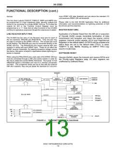
DIFFERENTIAL
AMPLIFIERS
COMPARATORS
VDD
RINA-40
RINA
ONE
PRIORITYLABELS
NULL
ZERO
The three Priority Label Registers store received data if the Priority
Label feature is enabled, and the incoming ARINC 429 word’s label
byte matches the value stored in Pririty-Label Match Register #1, # 2
or #3.
GND
VDD
RINB
Priority-Label capture is enabled by setting the Receive Control
Register PLON bit to “1”. When PLON = “0” the Priority-Label feature
is disabled and no ARINC 429 words are stored in the Priority-Label
Registers.
RINB-40
GND
FIGURE 2. ARINC RECEIVER INPUT
HOLT INTEGRATED CIRCUITS
10

 HOLTIC [ HOLT INTEGRATED CIRCUITS ]