HI-3593
FUNCTIONAL DESCRIPTION (cont.)
SELF TEST
TRANSMITTER
FIFO OPERATION
If Transmit Control Register bit SELFTEST is equal ”1”, the
transmitter serial output data is internally looped-back into the
Figure 4 shows a block diagram of the HI-3593 transmitter. The receiver 1. The data will appear inverted (compliment) on receiver 2.
Transmit FIFO is loaded with ARINC 429 words awaiting Data passes unmodified from transmitter to receiver 1. Setting
transmission. SPI op-code 0x0C writes each ARINC 429 word into Transmit Control register bit SELFTEST to ”1” forces TXAOUT and
the FIFO, at the next available FIFO location. If Transmit Status TXBOUT to the Null state to prevent self-test data from appearing on
Register bit TFEMPTY equals “1” (FIFO empty), then up to 32 words theARINC 429 bus.
(32 bits each) may be loaded. If Transmit Status Register bit
TFEMPTY equals “0” then only the available positions may be
loaded. If all 32 positions are full, Transmit Status Register bit
TFFULL is asserted. Further attempts to load the Transmit FIFO are
ignored until at least oneARINC 429 word is transmitted.
SYSTEM OPERATION
The receivers are independent of the transmitter. Therefore,
control of data exchanges is strictly at the option of the user. The
only restrictions are:
The Transmit FIFO half-full flag (Transmit Status Register bit
TFHALF) equals “0” when the Transmit FIFO contains less than 16
words. When TFHALF equals “0”, the system microprocessor can
safely initiate a 16-word ARINC 429 write sequence.
1. The received data will be overwritten if the Receive FIFO is
full and at least one location is not retrieved before the next
complete ARINC 429 word is received.
In normal operation (Transmit Control Register bit TPARITY = ”1”),
the 32nd bit transmitted is an odd parity bit. If Transmit Control
Register bit PARITY equals “0”, all 32 bits loaded into the Transmit
FIFO are treated as data and are transmitted.
2. The Transmit FIFO can store 32 words maximum and
ignores attempts to load additional data when full.
DC/DC CONVERTER
The Transmit and Receive FIFOs may be cleared using Software
Reset (SPI op-code 0x44). The Transmit FIFO should be cleared
after a self-test before starting normal operation to avoid inadvertent
transmission of test data.
The HI-3593 requires only a single +3.3V power supply. An
integrated inverting / non-inverting voltage doubler generates the
rail voltages (+/- 6.6V) which then power the line driver to produce
the required +/- 5VARINC 429 signal levels.
DATATRANSMISSION
The internal dual-polarity charge pump requires four external
capacitors, two for each polarity generated by the doubler. Pins CP+
and CP- connect the external “fly” capacitor, CFLY, to the positive
portion of the doubler, resulting in twice VDD at the V+ pin. An output
“hold” capacitor, COUT, is placed between V+ and GND. COUT
should be ten times the size of CFLY. The inverting negative portion
of the converter works in a similar fashion, with CFLY and COUT
placed between CN+ / CN- and V- / GND respectively. Note that low
ESR capacitors should be used. Recommended values are given in
the block diagram on page 2.
If Transmit Control Register bit TMODE equals “1”, ARINC 429 data
is transmitted immediately following the CS rising edge of the SPI
instruction that loaded data into the Transmit FIFO. Writing Transmit
Control Register bit TMODE to “0” allows the software to control
transmission timing; each time an SPI op-code 0x40 is executed, all
loaded Transmit FIFO words are transmitted. If new words are
loaded into the Transmit FIFO before transmission stops, the new
words will also be output. Once the Transmit FIFO is empty and
transmission of the last word is complete, the FIFO can be loaded
with new data which is held until the next SPI 0x40 instruction is
executed. Once transmission is enabled, the FIFO positions are
incremented with the top register loading into the data transmission
shift register. Within 2.5 data clocks the first data bit appears at
TXAOUT and TXBOUT. The 31 or 32 bits in the data transmission
shift register are presented sequentially to the outputs in the ARINC
429 format with the following timing:
LINE DRIVER OPERATION
The line driver in the HI-3593 directly drives the ARINC 429 bus.
The two ARINC 429 outputs (TXAOUT and TXBOUT) provide a
differential voltage to produce a +10V One, a -10V Zero, and a 0 Volt
Null. Transmit Control Register bit RATE controls both the
transmitter data rate and the slope of the differential output signal.
No additional hardware is required to control the slope.
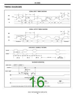
HIGH SPEED LOW SPEED
ARINC DATA BIT TIME
DATA BIT TIME
NULL BIT TIME
10 Clocks
5 Clocks
5 Clocks
40 Clocks
80 Clocks
40 Clocks
40 Clocks
320 Clocks
Writing Transmit Control Register bit RATE to “0” causes a 100
Kbit/s data rate and a slope of 1.5 µs on the ARINC 429 outputs.
Setting RATE to “1” causes a 12.5 Kbit/s data rate and a slope of
10µs. Slope rate is set by an on-chip resistor and capacitor and
tested to be withinARINC 429 specification requirements.
WORD GAP TIME
A word counter detects when all loaded positions have been
transmitted and sets the Transmit Status Register TFEMPTY bit
high.
LINE DRIVER OUTPUT PINS
TRANSMITTER PARITY
The HI-3593 TXAOUT and TXBOUT pins have 37.5 Ohms in series
with each line driver output, and may be directly connected to an
ARINC 429 bus. The alternate AMPA and AMPB pins have 5 Ohms
of internal series resistance and require external 32.5 ohm resistors
at each pin. AMPA and AMPB are for applications where external
series resistance is applied, typically for lightning protection
The parity generator counts the Ones in the 31-bit word. The 32nd
bit transmitted will make parity odd. Setting Transmit Control
Register bit TPARITY to “0” bypasses the parity generator, and
allows 32 bits of data to be transmitted.
HOLT INTEGRATED CIRCUITS
12

 HOLTIC [ HOLT INTEGRATED CIRCUITS ]