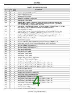
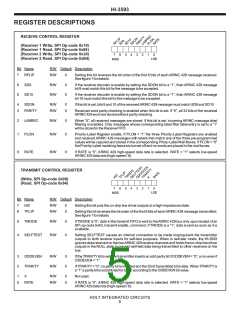
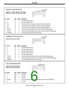
HI-3593
ARINC 429 BIT ORDERING
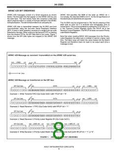
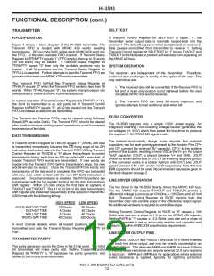
ARINC 429 messages consist of a 32-bit sequence as shown
below. The first eight bits that appear on the ARINC 429 bus are
the label byte. The next twenty three bits comprise a data field
which presents data in a variety of formats defined in the ARINC
429 specification. The last bit transmitted is an odd parity bit.
ARINC 429 specifies the MSB of the label as ARINC bit 1.
Conversely, the data field MSB is bit 31. So the bit significance of
the label byte and data fields are opposite.
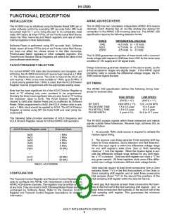
The HI-3593 may be programmed to “flip” the bit ordering of the
label byte as soon as it is received and immediately prior to
transmission. This is accomplished by setting the TFLIP bit to a “1”
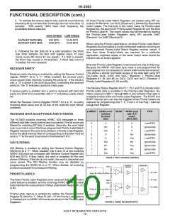
in the Transmit Control Register and/or the RFLIP bit in the
Receive Control Registers. The RFLIP bit does not control Priority
Label Match Registers.
ARINC 429 data is transmitted between the HI-3593 and host
microcontroller using the four-wire Serial Peripheral Interface
(SPI). A read or write operation consists of a single-byte op-code
followed by the data. When writing to the transmit FIFO or reading
from the receive FIFOs, the SPI data field is four bytes. Figure 1
shows how the SPI data bytes are mapped to the ARINC 429
message.
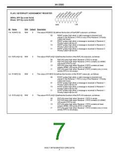
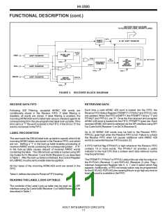
Note that when reading ARINC 429 messages from the Priority-
Label Registers the label byte is omitted to permit a faster read
time. The label value will match the value loaded into the Match
Register and therefore does not need to be output each time a
message is read.
ARINC 429 Message as received / transmitted on the ARINC 429 serial bus
MSB
LABEL
LSB
LSB
DATA
MSB
ARITY
P
1
2
3
4
5
6
7
8
9 10 11 12 13 14 15 16 17 18 19 20 21 22 23 24 25 26 27 28 29 30 31 32
time
ARINC 429 Message as transferred on the SPI bus
SPI Op-Code
MSB
ARITY
DATA
LSB
LSB
LABEL
MSB
P
0
0
0
0
1
1
0
0
32 31 30 29 28 27 26 25 24 23 22 21 20 19 18 17 16 15 14 13 12 11 10 9
8
7
6
3
5
4
3
6
2
1
Example 1. Write Transmit FIFO (Op-Code 0x0C) with TFLIP bit = “0”.
SPI Op-Code
MSB
ARITY
DATA
LSB
MSB
LABEL
LSB
P
1
0
1
0
0
0
0
0
32 31 30 29 28 27 26 25 24 23 22 21 20 19 18 17 16 15 14 13 12 11 10 9
1
2
4
5
7 8
Example 2. Read Receiver 1 FIFO (Op-Code 0xA0) with RFLIP bit = “1”.
SPI Op-Code
MSB
ARITY
DATA
LSB
P
1
1
0
0
1
1
0
0
32 31 30 29 28 27 26 25 24 23 22 21 20 19 18 17 16 15 14 13 12 11 10 9
Example 3. Read Receiver 2 Priority-Label Register #3 (Op-Code 0xCC).
SPI Op-Code
MSB LABEL #3 LSB
MSB LABEL #2 LSB
MSB LABEL #1 LSB
0
0
1
0
1
1
0
0
1
2
3
4
5
6
7
8
1
2
3
4
5
6
7
8
1 2 4
3 6 7 8
5
Example 4. Write Receiver 2 Priority-Label Match Registers (Op-Code 0x2C)with RFLIP bit = “1” or “0”.
FIGURE 1. ARINC 429 & SPI BIT ORDERING
HOLT INTEGRATED CIRCUITS
8

 HOLTIC [ HOLT INTEGRATED CIRCUITS ]