HI-3593
FUNCTIONAL DESCRIPTION (cont.)
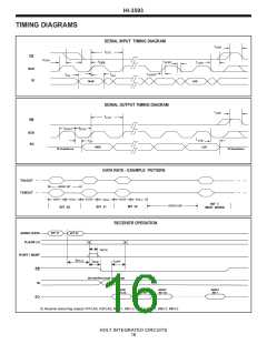
mum ARINC 429 data threshold and just above the standard 2.5
volt maximum ARINC 429 null threshold.
devices.
The line driver outputs TXAOUT, TXBOUT, AMPA and AMPB may
be programmed to a high impedance state, allowing multiple line
drivers to be connected to a single ARINC 429 bus. To tri-state the
outputs bit HIZ in the Transmit Control Register must be
programmed to a “1”. Note that all other functions of the HI-3593
continue to operate as usual even though the outputs are tri-stated.
Please refer to the Holt AN-300 Application Note for additional
information and recommendations on lightning protection of Holt
line drivers and line receivers.
MASTER RESET (MR)
LINE RECEIVER INPUT PINS
Application of a Master Reset from the MR pin or execution
of Opcode (0x04) causes immediate termination of data
transmission and reception and clears the receive control
registers, transmit control register, ACLK and Flag/Interrupt
Registers to the default states. All FIFOs will be emptied and
status flags are set to the default state (TFULL is reset,
TEMPTY is set). NOTE: Reading an EMPTY FIFO may
result in invalid data.
The HI-3593 has two sets of Line Receiver input pins for each of
the two receivers, RINxA/B and RINxA/B-40. Only one pair may
be used to connect to the ARINC 429 bus. The unused pair must
be left floating. The RINxA/B pins may be connected directly to the
ARINC 429 bus. The RINxA/B-40 pins require external 40K ohm
resistors in series with each ARINC input. These do not affect the
ARINC receiver thresholds. By keeping excessive voltage outside
the device, this option is helpful in applications where lightning pro-
tection is required.
SOFTWARE RESET
When using the RINxA/B-40 pins, each side of the ARINC 429 bus
must be connected through a 40K ohm series resistor in order for
the chip to detect the correct ARINC 429 levels. The typical 10 Volt
differential signal is translated and input to a window comparator
and latch. The comparator levels are set so that with the external
40K ohm resistors, they are just below the standard 6.5 volt mini-
Opcode (0x044) clears the transmit and receive FIFOs and
the Priority-Label Registers only. All other registers are
unaffected by Software Reset.
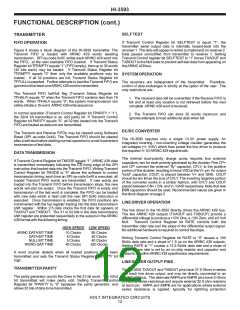
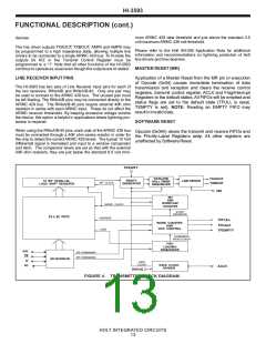
TPARITY
DATA AND
NULL TIMER
SEQUENCER
TXAOUT
TXBOUT
PARITY
GENERATOR
LINE DRIVER
32 BIT PARALLEL
LOAD SHIFT REGISTER
BIT CLOCK
HIZ
BIT
AND
WORD GAP
COUNTER
WORD CLOCK
START
SEQUENCE
32 x 32 FIFO
ADDRESS
LOAD
TFFULL
WORD COUNTER
AND
FIFO CONTROL
TFHALF
TFEMPTY
INCREMENT
WORD COUNT
FIFO
LOADING
SEQUENCER
SCK
CS
SI
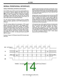
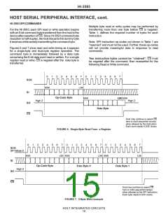
SPI COMMANDS
SPI COMMANDS
SPI INTERFACE
DATA
CLOCK
DATA CLOCK
DIVIDER
SO
ACLK
DIV[3:0]
FIGURE 4. TRANSMITTER BLOCK DIAGRAM
HOLT INTEGRATED CIRCUITS
13

 HOLTIC [ HOLT INTEGRATED CIRCUITS ]