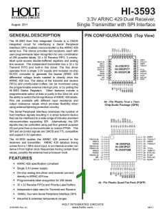
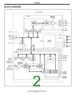
HI-3593
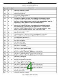
REGISTER DESCRIPTIONS
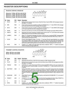
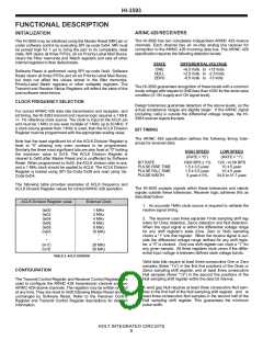
RECEIVE CONTROL REGISTER
TE
PLONRA
SD10
(Receiver 1 Write, SPI Op-code 0x10)
(Receiver 1 Read, SPI Op-code 0x94)
(Receiver 2 Write, SPI Op-code 0x24)
(Receiver 2 Read, SPI Op-code 0xB4)
7
6
5
4
3
2
1
0
LSB
MSB
Bit Name
R/W Default Description
7
6
5
RFLIP
R/W
R/W
R/W
0
0
0
Setting this bit reverses the bit order of the first 8 bits of each ARINC 429 message received.
See figure 1 for details.
SD9
If the receiver decoder is enable by setting the SDON bit to a “1”, then ARINC 429 message
bit 9 must match this bit for the message to be accepted.
SD10
If the receiver decoder is enable by setting the SDON bit to a “1”, then ARINC 429 message
bit 10 must match this bit for the message to be accepted.
4
3
SDON
R/W
R/W
0
0
If this bit is set, bits 9 and 10 of the receivedARINC 429 message must match SD9 and SD10
PARITY
Received word parity checking is enabled when this bit is set. If “0”, all 32 bits of the received
ARINC 429 word are stored without parity checking.
2
1
LABREC
PLON
R/W
R/W
0
0
When “0”, all received messages are stored. If this bit is set, incoming ARINC message label
filtering is enabled. Only messages whose corresponding label filter table entry is set to a “1”
will be stored in the Receive FIFO.
Priority-Label Register enable. If PLON = “1” the three Priority-Label Registers are enabled
and received ARINC 429 messages with labels that match one of the three pre-programmed
values will be capured and stored in the corresponding Prioty-Label Mail Boxes. If PLON = “0”
the Priority-Label matching feature is turned off and no words are placed in the mail boxes.
0
RATE
R/W
0
If RATE is “0”, ARINC 429 high-speed data rate is selected. RATE = “1” selects low-speed
ARINC 429 data rate (high-speed / 8).
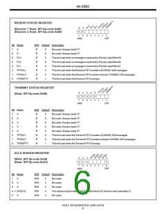
TRANSMIT CONTROL REGISTER
TE
RA
TMOD
S
E
ELFTEST
X
(Write, SPI Op-code 0x08)
(Read, SPI Op-code 0x84)
7
6
5
4
3
2
1
0
LSB
MSB
Bit Name
R/W Default Description
7
6
HIZ
R/W
R/W
0
0
Setting this bit puts the on-chip line driver outputs to a high-impedance state.
TFLIP
Setting this bit reverses the bit order of the first 8 bits of eachARINC 429 message transmitted.
See figure 1 for details.
5
4
TMODE
R/W
R/W
0
0
If TMODE is “0”, data in the transmit FIFO is sent to theARINC 429 bus only upon receipt of an
SPI op-code 0x40, transmit enable, command. If TMODE is a “1”, data is sent as soon as it is
available.
SELFTEST
Setting SELFTEST causes an internal connection to be made looping-back the transmitter
outputs to both receiver inputs for self-test purposes. When in self-test mode, the HI-3593
ignores data received on the twoARINC 429 receive channels and holds the on-chip line driver
outputs in the NULL state to prevent self-test data being transmitted to other receivers on the
bus.
3
2
ODDEVEN
TPARITY
R/W
R/W
0
0
If theTPARITYbit is set, the transmitter inserts an odd parity bit if ODDEVEN = “0”, or an even if
ODDEVEN = “1”.
IfTPARITY= “0”, no parity bit is inserted and the 32nd transmitted bit is data. WhenTPARITYis
a “1” a parity bit is substituted for bit 32 according to the ODDEVEN bit value.
1
0
X
R/W
R/W
0
0
Not used.
RATE
If RATE is “0”, ARINC 429 high-speed data rate is selected. RATE = “1” selects low-speed
ARINC 429 data rate (high-speed / 8).
HOLT INTEGRATED CIRCUITS
5

 HOLTIC [ HOLT INTEGRATED CIRCUITS ]