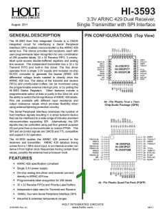
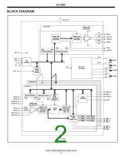
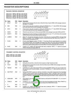
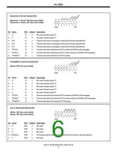
HI-3593
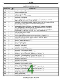
TABLE 1. DEFINED INSTRUCTIONS
DESCRIPTION
Op-Code R/W # Data
bytes
0x00
0x04
0x08
0x0C
0x10
0x14
W
W
W
W
W
W
0
0
Instruction not implemented. No operation.
Software controlled Master Reset
Write Transmit Control Register
1
4
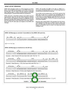
Write ARINC 429 message to Transmit FIFO
Write Receiver 1 Control Register
1
32
Write label values to Receiver 1 label memory. Starting with label 0xFF, consecutively set or reset each
label in descending order. For example, if the first data byte is programmed to 10110010 then labels FF,
FD FC and F8 will be set and FE, FB, FA and F7 will be reset.
0x18
W
3
Write Receiver 1 Priority-Label Match Registers. The data field consists of three eight-bit labels. The first data
byte is written to P-L filter #3, the second to P-L filter #2, and the last byte to filter #1
0x24
0x28
W
W
1
Write Receiver 2 Control Register
32
Write label values to Receiver 2 label memory. Starting with label 0xFF, consecutively set or reset each
label in descending order. For example, if the first data byte is programmed to 10110010 then labels FF,
FD FC and F8 will be set and FE, FB, FA and F7 will be reset.
0x2C
W
3
Write Receiver 2 Priority-Label Match Registers. The data field consists of three eight-bit labels. The first
eight bits is written to P-L filter #3, the second to P-L filter #2, and the last byte to filter #1
0x34
0x38
0x40
0x44
0x48
0x4C
0x80
0x84
0x90
0x94
0x98
0x9C
0xA0
0xA4
0xA8
0xAC
0xB0
0xB4
0xB8
0xBC
0xC0
0xC4
0xC8
0xCC
0xD0
0xD4
0xFF
W
W
W
W
W
W
R
R
R
R
R
R
R
R
R
R
R
R
R
R
R
R
R
R
R
R
R
1
1
0
0
0
0
1
1
1
1
32
3
4
3
3
3
1
1
32
3
4
3
3
3
1
1
0
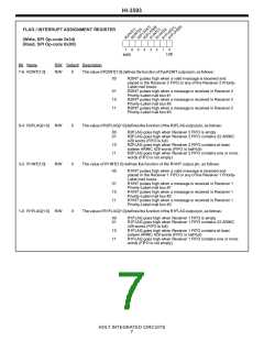
Write Flag / Interrupt Assignment Register
Write ACLK Division Register
Transmit current contents of Transmit FIFO if Transmit Control Register bit 5 (TMODE) is a “0”
Software Reset. Clears the Transmit and Receive FIFOs and the Priority-Label Registers
Set all bits in Receiver 1 label memory to a “1”
Set all bits in Receiver 2 label memory to a “1”
Read Transmit Status Register
Read Transmit Control Register
Read Receiver 1 Status Register
Read Receiver 1 Control Register
Read label values from Receiver 1 label memory.
Read Receiver 1 Priority-Label Match Registers.
Read one ARINC 429 message from the Receiver 1 FIFO
Read Receiver 1 Priority-Label Register #1, ARINC429 bytes 2,3 & 4 (bits 9 - 32)
Read Receiver 1 Priority-Label Register #2, ARINC429 bytes 2,3 & 4 (bits 9 - 32)
Read Receiver 1 Priority-Label Register #3, ARINC429 bytes 2,3 & 4 (bits 9 - 32)
Read Receiver 2 Status Register
Read Receiver 2 Control Register
Read label values from Receiver 2 label memory.
Read Receiver 2 Priority-Label Match Registers.
Read one ARINC 429 message from the Receiver 2 FIFO
Read Receiver 2 Priority-Label Register #1, ARINC429 bytes 2,3 & 4 (bits 9 - 32)
Read Receiver 2 Priority-Label Register #2, ARINC429 bytes 2,3 & 4 (bits 9 - 32)
Read Receiver 2 Priority-Label Register #3, ARINC429 bytes 2,3 & 4 (bits 9 - 32)
Read Flag / Interrupt Assignment Register
Read ACLK Division Register
Instruction not implemented. No operation.
HOLT INTEGRATED CIRCUITS
4

 HOLTIC [ HOLT INTEGRATED CIRCUITS ]