HI-3593
SERIAL PERIPHERAL INTERFACE
SERIALPERIPHERALINTERFACE (SPI) BASICS
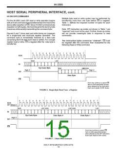
The SPI protocol transfers serial data as 8-bit bytes. Once
CS chip select is asserted, the next 8 rising edges on SCK
latch input data into the master and slave devices, starting
with each byte’s most-significant bit. The HI-3593 SPI can
be clocked at 10 MHz.
The HI-3593 uses an SPI synchronous serial interface for
host access to internal registers and data FIFOs. Host
serial communication is enabled through the Chip Select
(CS) pin, and is accessed via a three-wire interface
consisting of Serial Data Input (SI) from the host, Serial
Data Output (SO) to the host and Serial Clock (SCK). All
read / write cycles are completely self-timed.
Multiple bytes may be transferred when the host holds CS
low after the first byte transferred, and continues to clock
SCK in multiples of 8 clocks. A rising edge on CS chip
select terminates the serial transfer and reinitializes the
HI-3593 SPI for the next transfer. If CS goes high before a
full byte is clocked by SCK, the incomplete byte clocked
into the device SI pin is discarded.
The SPI (Serial Peripheral Interface) protocol specifies
master and slave operation; the HI-3593 operates as an
SPI slave.
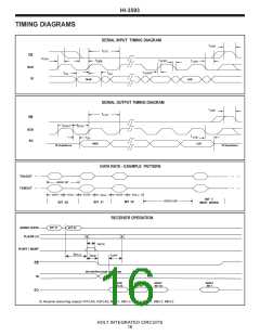
The SPI protocol defines two parameters, CPOL (clock
polarity) and CPHA (clock phase). The possible CPOL-
CPHA combinations define four possible "SPI Modes".
Without describing details of the SPI modes, the HI-3593
operates in mode 0 where input data for each device (
master and slave) is clocked on the rising edge of SCK,
and output data for each device changes on the falling
edge (CPHA = 0, CPOL = 0). Be sure to set the host SPI
logic for mode 0.
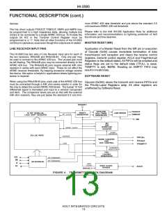
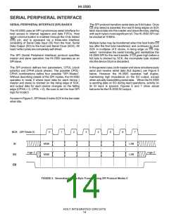
In the general case, both master and slave simultaneously
send and receive serial data (full duplex), per Figure 5
below. However the HI-3593 operates half duplex,
maintaining high impedance on the SO output, except
when actually transmitting serial data. When the HI-3593
is sending data on SO during read operations, activity on
its SI input is ignored. Figures 6 and 7 show actual
behavior for the HI-3593 SO output.
As seen in Figure 5, SPI Mode 0 holds SCK in the low state
when idle.
0
1
2
3
4
5
6
7
SCK (SPI Mode 0)
SI
MSB
LSB
LSB
High Z
High Z
SO
MSB
CS
FIGURE 5. Generalized Single-Byte Transfer Using SPI Protocol Modes 0
HOLT INTEGRATED CIRCUITS
14

 HOLTIC [ HOLT INTEGRATED CIRCUITS ]