HI-3593
HOST SERIAL PERIPHERAL INTERFACE, cont.
HI-3593 SPI COMMANDS
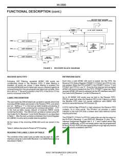
Multiple byte read or write cycles may be performed by
For the HI-3593, each SPI read or write operation begins
with an 8-bit command byte transferred from the host to the
device after assertion of CS. Since HI-3593 command byte
reception is half-duplex, the host discards the dummy byte
it receives while serially transmitting the command byte.
transferring more than one byte before CS is negated.
Table 1. defines the required number of bytes for each
instruction.
Note: SPI Instruction op-codes not shown in Table 1 are
“reserved” and must not be used. Further, these op-codes
will not provide meaningful data in response to read
commands.
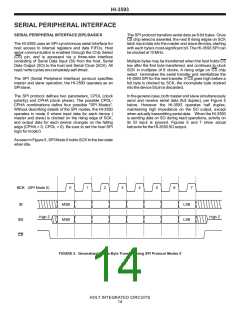
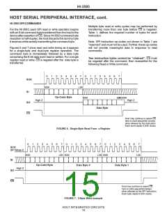
Figures 6 and 7 show read and write timing as it appears
for a single-byte and dual-byte register operation. The
command byte is immediately followed by a data byte
comprising the 8-bit data word read or written. For a single
register read or write, CS is negated after the data byte is
transferred.
Two instruction bytes cannot be “chained”; CS must
be negated after the command, then reasserted for the
following Read or Write command.
0
1
2
3
4
5
6
7
0
1
2
3
4
5
6
7
SCK
MSB
LSB
SI
Op-Code Byte
MSB
LSB MSB
High Z
High Z
SO
CS
Data Byte
Host may continue to assert CS
here to read sequential word(s)
when allowed by the instruction.
Each word needs 8 SCK clocks.
FIGURE 6. Single-Byte Read From a Register
0
1
2
3
4
5
6
7
0
1
2
3
4
5
6
7
0
1
2
3
4
5
6
7
SCK
SPI Mode 0
MSB
LSB MSB
LSB MSB
LSB
SI
Op-Code Byte
Data Byte 0
Data Byte 1
High Z
SO
CS
Host may continue to assert CS
here to write sequential byte(s)
when allowed by the SPI instruction.
Each byte needs 8 SCK clocks.
FIGURE 7. 2-Byte Write example
HOLT INTEGRATED CIRCUITS
15

 HOLTIC [ HOLT INTEGRATED CIRCUITS ]