Preliminary
HT45R04/HT45R04E
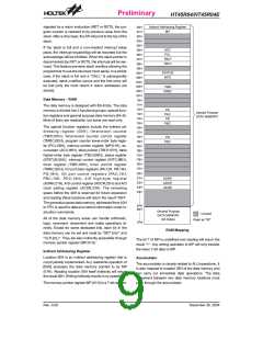
V
D
D
device by the options. Awakening from an I/O port stim-
ulus, the program will resume execution of the next in-
struction. If it awakens from an interrupt, two sequences
may occur. If the related interrupt is disabled or the inter-
rupt is enabled but the stack is full, the program will re-
sume execution at the next instruction. If the interrupt is
enabled and the stack is not full, a regular interrupt re-
sponse takes place. If an interrupt request flag is set to
²1² before entering the HALT mode, the wake-up func-
tion of the related interrupt will be disabled. Once a
wake-up event occurs, it takes 1024 tSYS (system clock
period) to resume normal operation. In other words, a
dummy period will be inserted after wake-up. If the
wake-up results from an interrupt acknowledge, the ac-
tual interrupt subroutine execution will be delayed by
one or more cycles. If the wake-up results in the next in-
struction execution, this will be executed immediately
after the dummy period is finished.
m
0 . 0 1 F *
1
0
0
k
R
E
S
1
0
k
m
0 . 1 F *
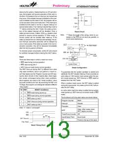
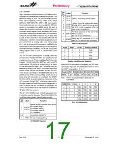
Reset Circuit
Note:
²*² Make the length of the wiring, which is con-
nected to the RES pin as short as possible, to
avoid noise interference.
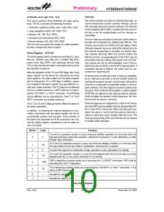
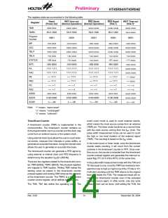
H
A
L
T
W
a
r
m
R
e
s
e
t
W
D
T
To minimize power consumption, all the I/O pins should
be carefully managed before entering the HALT status.
R
E
S
C
o
l
d
R
e
s
e
t
Reset
S
S
T
1
0
-
b
i
t
R
i
p
p
l
e
O
S
C
1
There are three ways in which a reset can occur:
C
o
u
n
t
e
r
·
·
·
RES reset during normal operation
RES reset during HALT
S
y
s
t
e
m
R
e
s
e
t
WDT time-out reset during normal operation
Reset Configuration
The WDT time-out during HALT is different from other
chip reset conditions, since it can perform a ²warm re -
set² that resets only the Program Counter and SP, leav-
ing the other circuits in their original state. Some regis-
ters remain unchanged during other reset conditions.
Most registers are reset to the ²initial condition² when
the reset conditions are met. By examining the PDF and
TO flags, the program can distinguish between different
²chip resets².
To guarantee that the system oscillator is started and
stabilized, the SST (System Start-up Timer) provides an
extra delay of 1024 system clock pulses when the sys-
tem resets (power-up, WDT time-out or RES reset) or
awakes from the HALT state.
When a system reset occurs, the SST delay is added
during the reset period. Any wake-up from HALT will en-
able the SST delay.
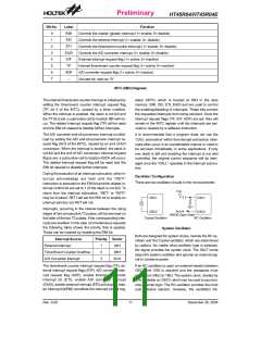
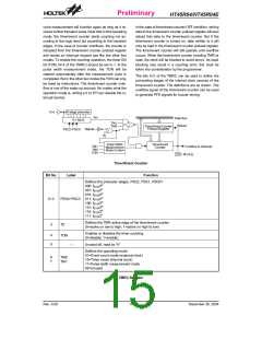
TO PDF
RESET Conditions
RES reset during power-up
RES reset during normal operation
RES wake-up HALT
An extra option load time delay is added during system
reset (power-up, WDT time-out at normal mode or RES
reset).
0
u
0
1
1
0
u
1
u
1
The functional unit chip reset status are shown below.
Program Counter
Interrupt
000H
WDT time-out during normal operation
WDT wake-up HALT
Disable
Clear
Prescaler
Note: ²u² means ²unchanged²
Clear. After master reset,
WDT begins counting
WDT
V
D
D
Timer/Event Counter Off
R
E
S
t
S
S
T
Input/Output Ports
SP
Input mode
Points to the top of the stack
S
S
T
T
i
m
e
-
o
u
t
C
h
i
p
R
e
s
e
t
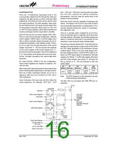
Reset Timing Chart
Rev. 0.00
13
December 30, 2004

 HOLTEK [ HOLTEK SEMICONDUCTOR INC ]