Preliminary
HT45R04/HT45R04E
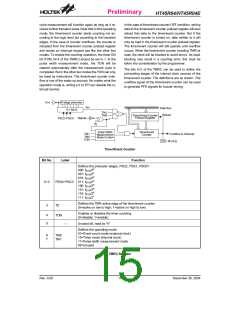
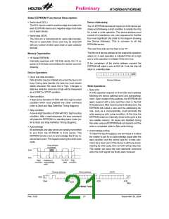
A/D Converter
Bit
No.
Label
Function
The 4 channels and 8-bit resolution A/D (7-bit accuracy)
converter are implemented in this microcontroller. The
reference voltage is VDD. The A/D converter contains
three special registers, namely, ADRH (21H) ADCR
(22H) and ACSR (23H). The ADRH is A/D result register
higher-order byte and are read-only. After the A/D con-
version is completed, the ADRH should be read to
retrieve the conversion result data. The ADCR is an A/D
converter control register, which defines the A/D chan-
nel number, analog channel select, start A/D conversion
control bit and end of A/D conversion flag. If users want
to start an A/D conversion, they should define the PB
configuration, select the converted analog channel, and
give START bit a raising edge and falling edge
(0®1®0). At the end of A/D conversion, the EOCB bit is
cleared and an A/D converter interrupt occurs (if the A/D
converter interrupt is enabled). The ACSR is A/D clock
setting register, which is used to select the A/D clock
source.
0
1
2
ACS0
ACS1 Defines the analog channel select.
ACS2
Defines the port B configuration select.
3
4
5
PCR0
If PCR0, PCR1 and PCR2 are all zero,
PCR1
the ADC circuit is powered off to re-
PCR2
duce power consumption.
Provides response at the end of the
EOCB A/D conversion.
6
7
(0= end of A/D conversion)
Starts the A/D conversion. (0®1®0=
START
start; 0®1= reset the A/D converter)
ADCR (22H) Register
ACS2
ACS1
ACS0
Analog Channel
0
0
0
0
0
0
1
1
0
1
0
1
AN0
AN1
AN2
AN3
The A/D converter control register is used to control the
A/D converter. The bit2~bit0 of the are used to select an
analog input channel. There are a total of eight channels
to select. The bit5~bit3 of the ADCRare used to set PB
configurations. PB can be an analog input or as digital
I/O line determined by these 3 bits. Once a PB line is se-
lected as an analog input, the I/O functions and pull-high
resistor of this I/O line are disabled and the A/D con-
verter circuit is powered on. The EOCB bit (bit6 of the
ADCR) is end of A/D conversion flag. Check this bit to
know when A/D conversion is completed. The START
bit of the ADCR is used to begin the conversion of the
A/D converter. Giving START bit a rising edge and fall-
ing edge means that the A/D conversion has started. In
order to ensure that A/D conversion is completed, the
START should remain at ²0² until the EOCB is cleared to
²0² (end of A/D conversion).
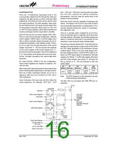
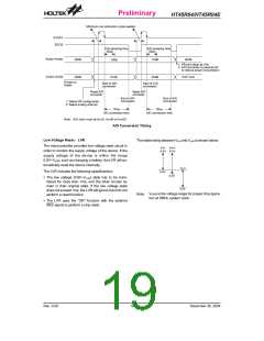
Analog Input Channel Selection
When the A/D conversion is completed, the A/D inter-
rupt request flag is set. The EOCB bit is set to ²1² when
the START bit is set from ²0² to ²1².
Register Bit7 Bit6 Bit5 Bit4 Bit3 Bit2 Bit1 Bit0
ADRH
D7 D6 D5 D4 D3 D2 D1 D0
Note: D0~D7 is A/D conversion result data bit
LSB~MSB.
PCR2 PCR1 PCR0
3
2
1
0
0
0
0
0
1
0
0
0
1
PB3
PB3
PB3
PB3
PB2
PB2
PB2
PB1
PB1
PB0
AN0
The bit 7 of the ACSR is used for testing purposes only.
It cannot be used by the users. The bit1 and bit0 of the
ACSR are used to select the A/D clock sources.
1
0
AN1 AN0
1
1
AN2 AN1 AN0
AN3 AN2 AN1 AN0
¾
¾
Bit
No.
Label
Function
Port B Configuration
Selects the A/D converter clock source
00= system clock/2
0
1
ADCS0
ADCS1
01= system clock/8
10= system clock/32
11= undefined
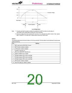
2~6
7
¾
Unused bit, read as ²0²
TEST For test mode used only
ACSR (23H) Register
Rev. 0.00
17
December 30, 2004

 HOLTEK [ HOLTEK SEMICONDUCTOR INC ]