Preliminary
HT45R04/HT45R04E
signaled by a return instruction (RET or RETI), the pro-
gram counter is restored to its previous value from the
stack. After a chip reset, the SP will point to the top of the
stack.
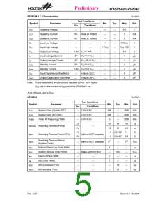
I
n
d
i
r
e
c
t
A
d
d
r
e
s
s
i
n
g
R
e
g
i
s
t
e
r
0
0
0
0
0
0
0
0
0
0
0
1
2
3
4
5
6
7
8
9
H
H
H
H
H
H
H
H
H
H
M
P
I
n
d
i
r
e
c
t
A
d
d
r
e
M
s
s
i
n
g
R
e
g
i
s
t
e
r
1
P
1
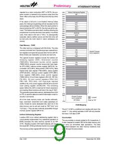
If the stack is full and a non-masked interrupt takes
place, the interrupt request flag will be recorded but the
acknowledge will be inhibited. When the stack pointer is
decremented (by RET or RETI), the interrupt will be ser-
viced. This feature prevents stack overflow allowing the
programmer to use the structure more easily. In a similar
case, if the stack is full and a ²CALL² is subsequently
executed, stack overflow occurs and the first entry will
be lost (only the most recent 4 return addresses are
stored).
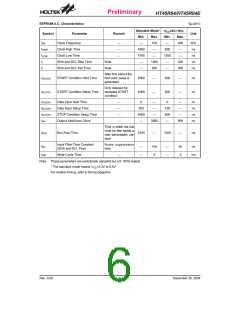
A
C
C
P
C
L
T
B
L
P
T
B
L
H
0
0
A
B
H
H
S
T
A
T
U
S
I
N
T
C
0
0
C
D
H
H
T
M
R
0
E
H
T
M
R
C
0
F
H
H
H
H
H
H
H
H
H
H
H
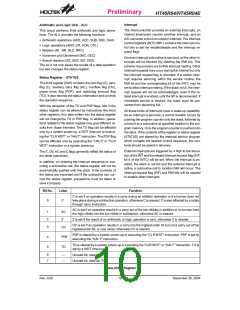
Data Memory - RAM
1
1
1
1
1
1
1
1
1
1
0
1
2
3
4
5
6
7
8
9
The data memory is designed with 85´8 bits. The data
memory is divided into 2 functional groups: special func-
tion registers and general purpose data memory (64´8).
Most of them are read/write, but some are read only.
P
A
S
p
e
c
i
a
l
P
u
r
p
o
s
e
P
A
C
D
A
T
A
M
E
M
O
R
Y
P
B
P
B
C
The special function registers include the indirect ad-
dressing register (00H), timer/event counter
(TMR;0DH), timer/event counter control register
(TMRC;0EH), program counter lower-order byte regis-
ter (PCL;06H), memory pointer register (MP;01H), ac-
cumulator (ACC;05H), table pointer (TBLP;07H), table
higher-order byte register (TBLH;08H), status register
(STATUS;0AH), interrupt control register (INTC;0BH),
timer register (TMR;0DH), timer control register
(TMRC;0EH), I/O port data registers (PA;12H, PB;14H,
PD;18H), I/O port control registers (PAC;13H,
PBC;15H, PDC;19H), A/D high-byte register
(ADRH;21H), A/D control register (ADCR;22H) and A/D
clock setting register (ACSR;23H). The remaining
space before the 40H is reserved for future expansion
and reading these locations will return the result ²00H².
The general purpose data memory, addressed from 40H
to 7FH, is used for data and control information under in-
struction commands.
P
D
P
D
C
1
1
A
B
H
H
1
1
C
D
H
H
1
E
H
1
F
H
H
H
H
H
H
2
2
2
2
2
0
1
2
3
4
A
A
D
D
R
C
H
R
A
C
S
R
3
F
H
4
0
H
G
e
n
e
r
a
l
P
u
r
p
o
s
e
:
U
n
u
s
e
d
D
A
T
A
M
E
M
O
R
Y
All of the data memory areas can handle arithmetic,
logic, increment, decrement and rotate operations di-
rectly. Except for some dedicated bits, each bit in the
data memory can be set and reset by ²SET [m].i² and
²CLR [m].i². They are also indirectly accessible through
memory pointer register (MP;01H).
(
6
4
B
y
t
e
s
)
R
e
a
d
a
s
"
0
0
"
7
F
H
RAM Mapping
The bit 7 of MP is undefined and reading will return the
result ²1². Any writing operation to MP will only transfer
the lower 7-bit data to MP.
Indirect Addressing Register
Location 00H is an indirect addressing register that is
not physically implemented. Any read/write operation of
[00H] accesses the data memory pointed to by MP
(01H). Reading location 00H itself indirectly will return
the result 00H. Writing indirectly results in no operation.
Accumulator
The accumulator is closely related to ALU operations. It
is also mapped to location 05H of the data memory and
can carry out immediate data operations. The data
movement between two data memory locations must
pass through the accumulator.
The memory pointer register MP (01H) is a 7-bit register.
Rev. 0.00
9
December 30, 2004

 HOLTEK [ HOLTEK SEMICONDUCTOR INC ]