Preliminary
HT45R04/HT45R04E
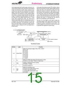
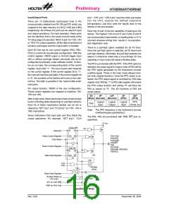
Input/Output Ports
[m].i², ²CPL [m]², ²CPLA [m]² read the entire port states
into the CPU, execute the defined operations
(bit-operation), and then write the results back to the
latches or the accumulator.
There are 13 bidirectional input/output lines in the
microcontroller, labeled from PA, PB and PD, which are
mapped to the data memory of [12H], [14H] and [18H]
respectively. All of these I/O ports can be used for input
and output operations. For input operation, these ports
are non-latching, that is, the inputs must be ready at the
T2 rising edge of instruction ²MOV A,[m]² (m=12H, 14H
or 18H). For output operation, all the data is latched and
remains unchanged until the output latch is rewritten.
Each line of port A has the capability of waking-up the
device. The highest 7-bit of port D and 4 bits of port B
are not physically implemented, on reading them a ²0² is
returned whereas writing then results in no-operation.
See Application note.
There is a pull-high option available for all I/O lines.
Once the pull-high option is selected, all I/O lines have
pull-high resistors. Otherwise, the pull-high resistors are
absent. It should be noted that a non-pull-high I/O line
operating in input mode will cause a floating state.
Each I/O line has its own control register (PAC, PBC,
PDC) to control the input/output configuration. With this
control register, CMOS output or Schmitt trigger input
with or without pull-high resistor structures can be re-
configured dynamically under software control. To func-
tion as an input, the corresponding latch of the control
register must write ²1². The input source also depends
on the control register. If the control register bit is ²1²,
the input will read the pad state. If the control register bit
is ²0², the contents of the latches will move to the inter-
nal bus. The latter is possible in the ²read-modify-write²
instruction.
The PA3 is pin-shared with the PFD. If the PFD option is
selected, the output signal in output mode of PA3 will be
the PFD signal generated by the timer/event counter
overflow signal. Those in the input mode always main-
tain their original functions. Once the PFD option is se-
lected, the PFD output signal is controlled by PA3 data
register only. Writing ²1² to PA3 data register will enable
the PFD output function and writing ²0² will force the
PA3 to remain at ²0². The I/O functions of PA3 are
shown below.
For output function, CMOS is the only configuration.
These control registers are mapped to locations 13H,
15H and 19H.
I/O
I/P
O/P
Mode (Normal) (Normal)
I/P
(PFD)
O/P
(PFD)
After a chip reset, these input/output lines remain at high
levels or floating state (depending on pull-high options).
Each bit of these input/output latches can be set or
cleared by ²SET [m].i² and ²CLR [m].i² (m=12H, 14H or
18H) instructions.
Logical
Input
Logical
Output
Logical
Input
PFD
PA3
(Timer on)
Note: The PFD frequency is the timer/event counter
overflowfrequencydividedby2.
Some instructions first input data and then follow the
The PA4, PA5 are pin-shared with TMR, INT pins re-
spectively.
output operations. For example, ²SET [m].i², ²CLR
V
D
D
C
o
n
t
r
o
l
B
i
t
P
U
D
Q
D
a
t
a
B
u
s
W
r
i
t
e
C
o
n
t
r
o
l
R
e
g
i
s
t
e
r
C
K
P
A
0
~
P
A
2
Q
P
A
3
/
P
F
D
S
C
h
i
p
R
e
s
e
t
P
A
4
/
/
T
I
M
R
P
P
A
A
5
6
7
0
N
T
R
e
a
d
C
o
n
t
r
o
l
R
e
g
i
s
t
e
r
P
A
/
/
S
A
D
N
A
D
a
t
a
B
i
t
P
B
0
~
P
B
3
/
A
N
3
D
C
Q
P
D
0
/
S
C
L
K
Q
W
r
i
t
e
D
a
t
a
R
e
g
i
s
t
e
r
S
M
U
P
A
3
X
P
F
D
P
F
D
E
N
M
(
P
A
3
)
U
X
R
e
a
d
D
a
t
a
R
e
g
i
s
t
e
r
S
y
s
t
e
m
W
a
k
e
-
u
p
O
P
0
~
O
P
7
(
P
A
o
n
l
y
)
I
N
T
f
o
r
P
A
A
5
O
O
n
n
l
y
y
T
M
R
f
o
r
P
4
l
Input/Output Ports
Rev. 0.00
16
December 30, 2004

 HOLTEK [ HOLTEK SEMICONDUCTOR INC ]