FT2232C Dual USB UART / FIFO I.C.
Pins go to 0x55 and then to 0xAA
Data read = 0xFF,0x55
(2) Pins start at 0xFF
Send 0x55,0xAA,0xAA
(repeat the last byte sent)
Pins go to 0x55 and then to 0xAA
Data read = 0xFF,0x55,0xAA
Enabling
Synchronous Bit-Bang mode is enabled using Set Bit Bang Mode driver command. A hex value of 4 will enable it, and
a hex value of 0 will reset the device. See application note AN2232C-02, “Bit Mode Functions for the FT2232C” for
more details and examples.
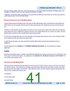
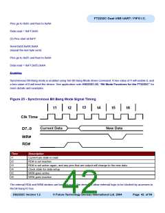
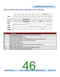
Figure 25 - Synchronous Bit Bang Mode Signal Timing
t3
t1
t2
t4
t5
t6
Clk Time
D7..0
Current Data
New Data
WR#
RD#
Time
t1
Description
Current pin state is read
RD# is set inactive
t2
t3
RD# is set active again, and any pins that are output will change to the new data.
t4
Clock state for data setup
WR# goes active
t5
t6
WR# goes inactive
The internal RD# and WR# strobes are brought out of the device to allow external logic to be clocked by accesses to
the bit-bang IO bus.
DS2232C Version 1.2
© Future Technology Devices International Ltd. 2004
Page 42 of 54

 FTDI [ FUTURE TECHNOLOGY DEVICES INTERNATIONAL LTD. ]