FT2232C Dual USB UART / FIFO I.C.
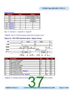
9.5 Enhanced Asynchronous and Synchronous Bit-Bang Modes - Signal Description and
Interface Configuration
Bit-bang mode is a special FT2232C device mode that changes the 8 IO lines on either (or both) channels into an 8
bit bi-directional data bus. The are two types of bit bang mode for the FT2232C - Enhanced Asynchronous Bit-Bang
Mode, which is virtually the same as FTDI BM chip-style Bit-Bang mode, with the addition of Read and Write strobes;
and Synchronous Bit-Bang mode, where data is only read from the device when the device is written to. Bit-Bang
mode is enabled by driver command. When either Channel A or Channel B (or both) have Enhanced Asynchronous
Bit-Bang mode, or Synchronous Bit-Bang mode enabled the IO signal lines are configured as follows :-
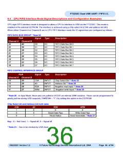
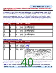
BIT-BANG DATA BUS GROUP **Note 24
Pin#
Signal
Type
Description
Channel A Channel B
24
23
22
21
20
19
17
16
40
39
38
37
36
35
33
32
D0
D1
D2
D3
D4
D5
D6
D7
I or O
I or O
I or O
I or O
I or O
I or O
I or O
I or O
Bit-Bang Data Bus Bit 0
Bit-Bang Data Bus Bit 1
Bit-Bang Data Bus Bit 2
Bit-Bang Data Bus Bit 3
Bit-Bang Data Bus Bit 4
Bit-Bang Data Bus Bit 5
Bit-Bang Data Bus Bit 6
Bit-Bang Data Bus Bit 7
BIT-BANG CONTROL INTERFACE GROUP
Pin#
Signal
Type
Description
Channel A Channel B
15
13
12
11
10
30
29
28
27
26
WR#
RD#
OUTPUT **Note 25
OUTPUT **Note 25
OUTPUT **Note 26
OUTPUT **Note 26
WR#
RD#
SI/WU
INPUT
The Send Immediate / WakeUp signal combines two functions
on a single pin. If USB is in suspend mode (PWREN# = 1) and
remote wakeup is enabled in the EEPROM , strobing this pin
low will cause the device to request a resume on the USB Bus.
Normally, this can be used to wake up the Host PC.
During normal operation (PWREN# = 0), if this pin is strobed low
any data in the device TX buffer will be sent out over USB on the
next Bulk-IN request from the drivers regardless of the pending
packet size. This can be used to optimise USB transfer speed for
some applications. Tie this pin to VCCIO if not used.
**Note 24 : In Input Mode, these pins are pulled to VCCIO via internal 200K resistors. These can be programmed to
gently pull low during USB suspend ( PWREN# = “1” ) by setting this option in the EEPROM.
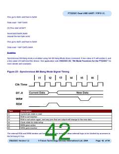
**Note 25 : The Bit-Bang Mode (synchronous and asynchronous) WR# and RD# strobes are on these pins when
DS2232C Version 1.2
© Future Technology Devices International Ltd. 2004
Page 40 of 54

 FTDI [ FUTURE TECHNOLOGY DEVICES INTERNATIONAL LTD. ]