FT2232C Dual USB UART / FIFO I.C.
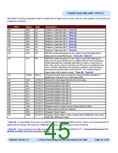
When MCU Host Bus Emulation mode is enabled the IO signal lines on both channels work together and the pins are
configured as follows :-
Pin#
Signal
AD0
AD1
AD2
AD3
AD4
AD5
AD6
AD7
I/O0
Type
I/O
I/O
I/O
I/O
I/O
I/O
I/O
I/O
I/O
Description
24
23
22
21
20
19
17
16
15
Address / Data Bus Bit 0 **Note 28
Address / Data Bus Bit 1 **Note 28
Address / Data Bus Bit 2 **Note 28
Address / Data Bus Bit 3 **Note 28
Address / Data Bus Bit 4 **Note 28
Address / Data Bus Bit 5 **Note 28
Address / Data Bus Bit 6 **Note 28
Address / Data Bus Bit 7 **Note 28
MPSSE mode instructions to set / clear or read the high byte of
data can be used with this pin. **Note 28, **Note 29
13
I/O1
I/O
MPSSE mode instructions to set / clear or read the high byte of
data can be used with this pin. In addition this pin has instructions
which will make the controller wait until it is high, or wait until it is
low. This can be used to connect to an IRQ pin of a peripheral chip.
The FT2232C will wait for the interrupt, and then read the device,
and pass the answer back to the host PC. I/O1 must be held in
input mode if this option is used. **Note 28, **Note 29
12
IORDY
INPUT
Extends the time taken to perform a Read or Write operation if
pulled low. Pull up to Vcc if not being used.
11
40
39
38
37
36
35
33
32
30
29
28
27
OSC
A8
OUTPUT Shows the clock signal that the circuit is using.
OUTPUT Extended Address Bus Bit 8
A9
OUTPUT Extended Address Bus Bit 9
A10
A11
A12
A13
A14
A15
CS#
ALE
RD#
WR#
OUTPUT Extended Address Bus Bit 10
OUTPUT Extended Address Bus Bit 12
OUTPUT Extended Address Bus Bit 13
OUTPUT Extended Address Bus Bit 14
OUTPUT Extended Address Bus Bit 15
OUTPUT Extended Address Bus Bit 16
OUTPUT Negative pulse to select device during Read or Write.
OUTPUT Positive pulse to latch the address.
OUTPUT Negative Read Output.
OUTPUT Negative Write Output. (Data is setup before WR# goes low, and is
held after WR# goes high)
**Note 28 : In Input Mode, these pins are pulled to VCCIO via internal 200K resistors. These can be programmed to
gently pull low during USB suspend ( PWREN# = “1” ) by setting this option in the EEPROM.
**Note 29 : These instrucions are fully described in the application note AN2232C-01 - “Command Processor For
MPSSE and MCU Host Bus Emulation Modes”.
DS2232C Version 1.2
© Future Technology Devices International Ltd. 2004
Page 45 of 54

 FTDI [ FUTURE TECHNOLOGY DEVICES INTERNATIONAL LTD. ]