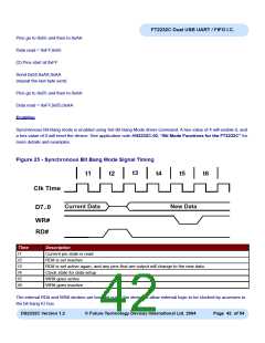
FT2232C Dual USB UART / FIFO I.C.
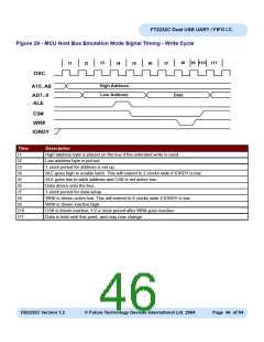
Figure 29 - MCU Host Bus Emulation Mode Signal Timing - Write Cycle
t3
t8 t9 t10 t11
t1
t2
t4
t5
t6
t7
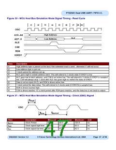
OSC
High Address
Low Address
A15..A8
Data
AD7..0
ALE
CS#
WR#
IORDY
Time
t1
Description
High address byte is placed on the bus if the extended write is used.
Low address byte is put out.
t2
t3
1 clock period for address is set up.
t4
ALE goes high to enable latch. This will extend to 2 clocks wide if IORDY is low.
ALE goes low to latch address and CS# is set active low.
Data driven onto the bus.
t5
t6
t7
1 clock period for data setup.
t8
WR# is driven active low. This will extend to 6 clocks wide if IORDY is low.
WR# is driven inactive high.
t9
t10
t11
CS# is driven inactive, 1/2 a clock period after WR# goes inactive
Data is held until this point, and may now change
DS2232C Version 1.2
© Future Technology Devices International Ltd. 2004
Page 46 of 54

 FTDI [ FUTURE TECHNOLOGY DEVICES INTERNATIONAL LTD. ]