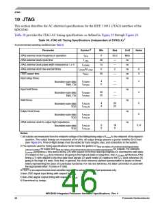
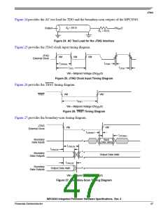
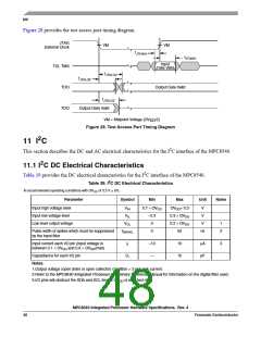
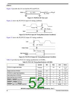
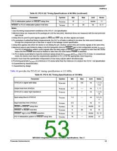
PCI/PCI-X
2
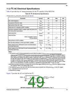
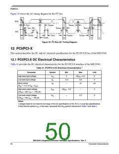
Figure 30 shows the AC timing diagram for the I C bus.
SDA
tI2CF
tI2CL
tI2DVKH
tI2KHKL
tI2CF
tI2SXKL
tI2CR
SCL
tI2SXKL
tI2CH
tI2SVKH
tI2PVKH
tI2DXKL
S
Sr
P
S
2
Figure 30. I C Bus AC Timing Diagram
12 PCI/PCI-X
This section describes the DC and AC electrical specifications for the PCI/PCI-X bus of the MPC8540.
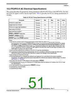
12.1 PCI/PCI-X DC Electrical Characteristics
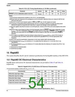
Table 41 provides the DC electrical characteristics for the PCI/PCI-X interface of the MPC8540.
1
Table 41. PCI/PCI-X DC Electrical Characteristics
Parameter
Symbol
Min
Max
Unit
High-level input voltage
Low-level input voltage
VIH
VIL
IIN
2
OVDD + 0.3
V
V
–0.3
—
0.8
5
Input current
(VIN 2 = 0 V or VIN = VDD
μA
)
High-level output voltage
VOH
OVDD – 0.2
—
—
V
V
(OVDD = min, IOH = –100 μA)
Low-level output voltage
VOL
0.2
(OVDD = min, IOL = 100 μA)
Notes:
1.Ranges listed do not meet the full range of the DC specifications of the PCI 2.2 Local Bus Specifications.
2.Note that the symbol VIN, in this case, represents the OVIN symbol referenced in Table 1 and Table 2.
MPC8540 Integrated Processor Hardware Specifications, Rev. 4
50
Freescale Semiconductor

 FREESCALE [ Freescale ]