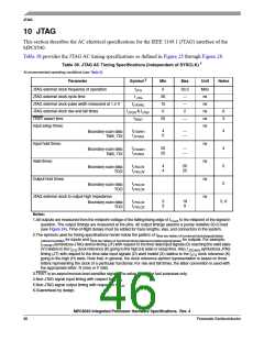
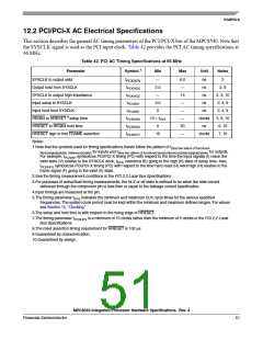
JTAG
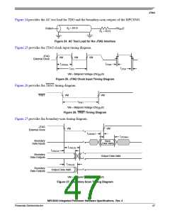
Figure 24 provides the AC test load for TDO and the boundary-scan outputs of the MPC8540.
Z0 = 50 Ω
OVDD/2
Output
RL = 50 Ω
Figure 24. AC Test Load for the JTAG Interface
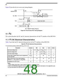
Figure 25 provides the JTAG clock input timing diagram.
JTAG
External Clock
VM
tJTKHKL
VM
VM
tJTGR
tJTGF
tJTG
VM = Midpoint Voltage (OV /2)
DD
Figure 25. JTAG Clock Input Timing Diagram
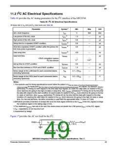
Figure 26 provides the TRST timing diagram.
TRST
VM
VM
tTRST
VM = Midpoint Voltage (OV /2)
DD
Figure 26. TRST Timing Diagram
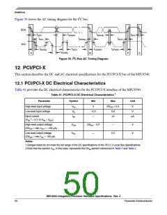
Figure 27 provides the boundary-scan timing diagram.
JTAG
VM
VM
External Clock
tJTDVKH
tJTDXKH
Boundary
Data Inputs
Input
Data Valid
tJTKLDV
tJTKLDX
Boundary
Data Outputs
Output Data Valid
tJTKLDZ
Output Data Valid
Boundary
Data Outputs
VM = Midpoint Voltage (OV /2)
DD
Figure 27. Boundary-Scan Timing Diagram
MPC8540 Integrated Processor Hardware Specifications, Rev. 4
Freescale Semiconductor
47

 FREESCALE [ Freescale ]