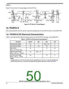
PCI/PCI-X
12.2 PCI/PCI-X AC Electrical Specifications
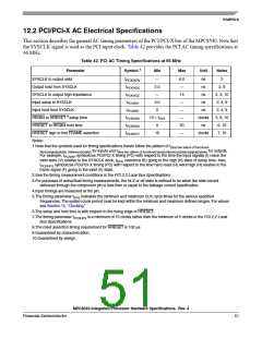
This section describes the general AC timing parameters of the PCI/PCI-X bus of the MPC8540. Note that
the SYSCLK signal is used as the PCI input clock. Table 42 provides the PCI AC timing specifications at
66 MHz.
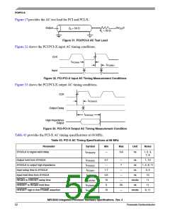
Table 42. PCI AC Timing Specifications at 66 MHz
Parameter
SYSCLK to output valid
Symbol 1
Min
Max
Unit
Notes
t
—
6.0
—
14
—
—
—
50
—
ns
ns
2
PCKHOV
Output hold from SYSCLK
SYSCLK to output high impedance
Input setup to SYSCLK
tPCKHOX
tPCKHOZ
tPCIVKH
tPCIXKH
tPCRVRH
tPCRHRX
tPCRHFV
2.0
2, 9
—
ns
2, 3, 10
2, 4, 9
2, 4, 9
5, 6, 10
6, 10
3.0
ns
Input hold from SYSCLK
0
ns
REQ64 to HRESET 9 setup time
HRESET to REQ64 hold time
HRESET high to first FRAME assertion
Notes:
10 × tSYS
clocks
ns
0
10
clocks
7, 10
1.Note that the symbols used for timing specifications herein follow the pattern of t(first two letters of functional
block)(signal)(state) (reference)(state) for inputs and t(first two letters of functional block)(reference)(state)(signal)(state) for outputs.
For example, tPCIVKH symbolizes PCI/PCI-X timing (PC) with respect to the time the input signals (I) reach the
valid state (V) relative to the SYSCLK clock, tSYS, reference (K) going to the high (H) state or setup time. Also,
tPCRHFV symbolizes PCI/PCI-X timing (PC) with respect to the time hard reset (R) went high (H) relative to the
frame signal (F) going to the valid (V) state.
2.See the timing measurement conditions in the PCI 2.2 Local Bus Specifications.
3.For purposes of active/float timing measurements, the Hi-Z or off state is defined to be when the total current
delivered through the component pin is less than or equal to the leakage current specification.
4.Input timings are measured at the pin.
5.The timing parameter tSYS indicates the minimum and maximum CLK cycle times for the various specified
frequencies. The system clock period must be kept within the minimum and maximum defined ranges. For values
see Section 15, “Clocking.”
6.The setup and hold time is with respect to the rising edge of HRESET.
7.The timing parameter tPCRHFV is a minimum of 10 clocks rather than the minimum of 5 clocks in the PCI 2.2 Local
Bus Specifications.
8.The reset assertion timing requirement for HRESET is 100 μs.
9.Guaranteed by characterization.
10.Guaranteed by design.
MPC8540 Integrated Processor Hardware Specifications, Rev. 4
Freescale Semiconductor
51

 FREESCALE [ Freescale ]