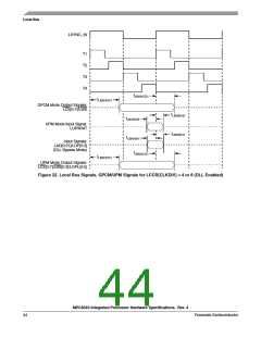
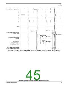
I2C
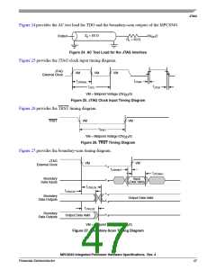
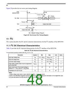
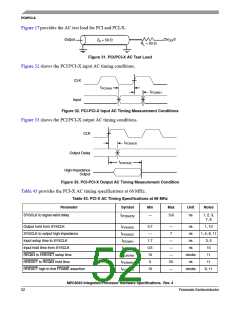
Figure 28 provides the test access port timing diagram.
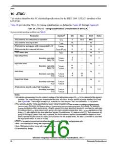
JTAG
VM
VM
External Clock
tJTIVKH
tJTIXKH
Input
Data Valid
TDI, TMS
tJTKLOV
tJTKLOX
TDO
Output Data Valid
tJTKLOZ
TDO
Output Data Valid
VM = Midpoint Voltage (OV /2)
DD
Figure 28. Test Access Port Timing Diagram
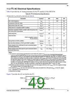
11 I2C
2
This section describes the DC and AC electrical characteristics for the I C interface of the MPC8540.
2
11.1 I C DC Electrical Characteristics
Table 39 provides the DC electrical characteristics for the I C interface of the MPC8540.
2
2
Table 39. I C DC Electrical Characteristics
At recommended operating conditions with OVDD of 3.3 V 5%.
Parameter
Input high voltage level
Symbol
Min
Max
Unit
Notes
VIH
VIL
0.7 × OVDD
OVDD+ 0.3
0.3 × OVDD
0.2 × OVDD
50
V
V
Input low voltage level
Low level output voltage
–0.3
0
VOL
V
1
2
Pulse width of spikes which must be suppressed
by the input filter
tI2KHKL
0
ns
Input current each I/O pin (input voltage is
between 0.1 × OVDD and 0.9 × OVDD(max)
II
–10
—
10
10
μA
3
Capacitance for each I/O pin
CI
pF
Notes:
1.Output voltage (open drain or open collector) condition = 3 mA sink current.
2.Refer to the MPC8540 Integrated Processor Preliminary Reference Manual for information on the digital filter used.
3.I/O pins will obstruct the SDA and SCL lines if OVDD is switched off.
MPC8540 Integrated Processor Hardware Specifications, Rev. 4
48
Freescale Semiconductor

 FREESCALE [ Freescale ]