PCI/PCI-X
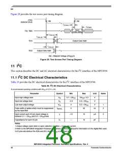
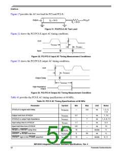
Figure 17 provides the AC test load for PCI and PCI-X.
OVDD/2
Output
Z0 = 50 Ω
RL = 50 Ω
Figure 31. PCI/PCI-X AC Test Load
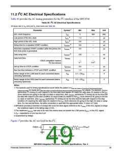
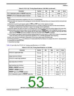
Figure 32 shows the PCI/PCI-X input AC timing conditions.
CLK
tPCIVKH
tPCIXKH
Input
Figure 32. PCI-PCI-X Input AC Timing Measurement Conditions
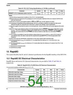
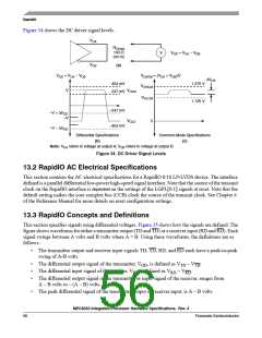
Figure 33 shows the PCI/PCI-X output AC timing conditions.
CLK
tPCKHOV
Output Delay
tPCKHOZ
High-Impedance
Output
Figure 33. PCI-PCI-X Output AC Timing Measurement Condition
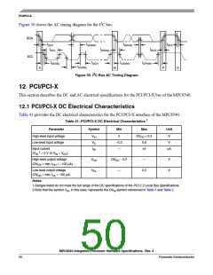
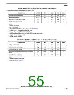
Table 43 provides the PCI-X AC timing specifications at 66 MHz.
Table 43. PCI-X AC Timing Specifications at 66 MHz
Parameter
SYSCLK to signal valid delay
Symbol
Min
Max
Unit
Notes
t
—
3.8
ns
1, 2, 3,
7, 8
PCKHOV
Output hold from SYSCLK
tPCKHOX
tPCKHOZ
tPCIVKH
tPCIXKH
tPCRVRH
tPCRHRX
tPCRHFV
0.7
—
—
7
ns
ns
1, 10
1, 4, 8, 11
3, 5
SYSCLK to output high impedance
Input setup time to SYSCLK
1.7
0.5
10
0
—
—
—
50
—
ns
Input hold time from SYSCLK
REQ64 to HRESET setup time
HRESET to REQ64 hold time
HRESET high to first FRAME assertion
ns
10
clocks
ns
11
11
10
clocks
9, 11
MPC8540 Integrated Processor Hardware Specifications, Rev. 4
52
Freescale Semiconductor

 FREESCALE [ Freescale ]