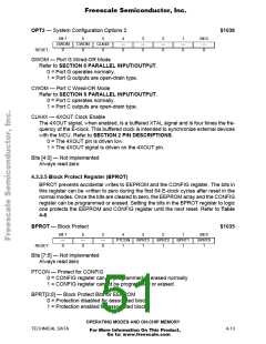
Freescale Semiconductor, Inc.
ADPU — A/D Power-Up
Refer to SECTION 10 ANALOG-TO-DIGITAL CONVERTER.
0 = A/D system disabled
1 = A/D system power enabled
CSEL — Clock Select
Selects alternate clock source for on-chip EEPROM and A/D charge pumps. On-chip
RC clock should be used when E clock falls below 1 MHz. Refer to SECTION 10 AN-
ALOG-TO-DIGITAL CONVERTER.
0 = A/D and EEPROM use system E clock
1 = A/D and EEPROM use internal RC clock
IRQE — Configure IRQ for Falling Edge-Sensitive Operation
Refer to SECTION 5 RESETS AND INTERRUPTS.
0 = Low level-sensitive operation.
1 = Falling edge-sensitive only operation.
DLY — Enable Oscillator Start-up Delay
Refer to SECTION 5 RESETS AND INTERRUPTS.
0 = The oscillator start-up delay coming out of STOP is bypassed and the MCU re-
sumes processing within about four bus cycles.
1 = A delay of approximately 4000 E-clock cycles is imposed as the MCU is started
up from the STOP power-saving mode.
CME — Clock Monitor Enable
In order to use both STOP and clock monitor, the CME bit must be written to zero be-
fore executing STOP, then written to one after recovering from STOP. Refer to SEC-
TION 5 RESETS AND INTERRUPTS.
0 = Clock monitor disabled
1 = Clock monitor enabled
FCME — Force Clock Monitor Enable
When FCME equals one, slow or stopped clocks will cause a clock failure reset. To
use STOP mode, FCME must always equal zero. Refer to SECTION 5 RESETS AND
INTERRUPTS.
0 = Clock monitor follows state of CME bit
1 = Clock monitor enabled and cannot be disabled until next reset
CR[1:0] — COP Timer Rate Select Bits
These control bits determine a scaling factor for the watchdog timer. Refer to SEC-
TION 5 RESETS AND INTERRUPTS.
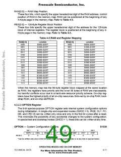
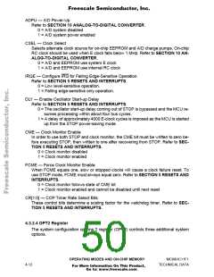
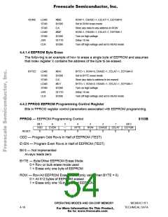
4.3.2.4 OPT2 Register
The system configuration options 2 register (OPT2) controls three additional system
options.
OPERATING MODES AND ON-CHIP MEMORY
MC68HC11F1
4-12
TECHNICAL DATA
For More Information On This Product,
Go to: www.freescale.com

 FREESCALE [ Freescale ]