Freescale Semiconductor, Inc.
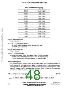
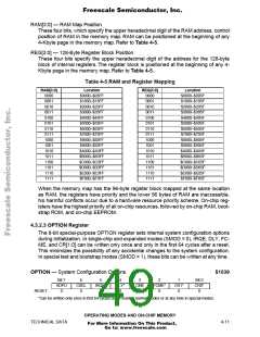
RAM[3:0] — RAM Map Position
These four bits, which specify the upper hexadecimal digit of the RAM address, control
position of RAM in the memory map. RAM can be positioned at the beginning of any
4-Kbyte page in the memory map. Refer to Table 4-5.
REG[3:0] — 128-Byte Register Block Position
These four bits specify the upper hexadecimal digit of the address for the 128-byte
block of internal registers. The register block is positioned at the beginning of any 4-
Kbyte page in the memory map. Refer to Table 4-5.
Table 4-5 RAM and Register Mapping
RAM[3:0]
0000
0001
0010
0011
0100
0101
0110
0111
1000
1001
1010
1011
1100
1101
1110
1111
Location
REG[3:0]
0000
0001
0010
0011
0100
0101
0110
0111
1000
1001
1010
1011
1100
1101
1110
1111
Location
$0000–$03FF
$1000–$13FF
$2000–$23FF
$3000–$33FF
$4000–$43FF
$5000–$53FF
$6000–$63FF
$7000–$73FF
$8000–$83FF
$9000–$93FF
$A000–$A3FF
$B000–$B3FF
$C000–$C3FF
$D000–$D3FF
$E000–$E3FF
$F000–$F3FF
$0000–$005F
$1000–$105F
$2000–$205F
$3000–$305F
$4000–$405F
$5000–$505F
$6000–$605F
$7000–$705F
$8000–$805F
$9000–$905F
$A000–$A05F
$B000–$B05F
$C000–$C05F
$D000–$D05F
$E000–$E05F
$F000–$F05F
When the memory map has the 96-byte register block mapped at the same location
as RAM, the registers have priority and the lower 96 bytes of RAM are inaccessible.
No harmful conflicts occur due to a hardware resource priority scheme. On-chip reg-
isters have the highest priority of all on-chip resources, followed by on-chip RAM, boot-
strap ROM, and on-chip EEPROM.
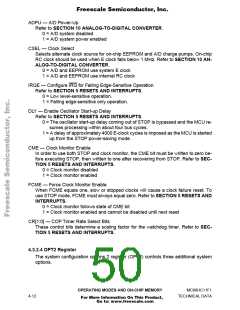
4.3.2.3 OPTION Register
The 8-bit special-purpose OPTION register sets internal system configuration options
during initialization. In single-chip and expanded modes (SMOD = 0), IRQE, DLY, FC-
ME, and CR[1:0] can be written only once and only in the first 64 cycles after a reset.
This minimizes the possibility of any accidental changes to the system configuration.
In special test and bootstrap modes (SMOD = 1), these bits can be written at any time.
OPTION — System Configuration Options
$1039
Bit 7
ADPU
0
6
CSEL
0
5
IRQE*
0
4
DLY*
0
3
CME
0
2
FCME*
0
1
CR1*
0
Bit 0
CR0*
0
RESET:
*Can be written only once in first 64 cycles out of reset in normal modes or at any time in special modes.
OPERATING MODES AND ON-CHIP MEMORY
TECHNICAL DATA
4-11
For More Information On This Product,
Go to: www.freescale.com

 FREESCALE [ Freescale ]