Freescale Semiconductor, Inc.
4.3.2 Initialization
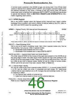
Because bits in the following registers control the basic configuration of the MCU, an
accidental change of their values could cause serious system problems. The protec-
tion mechanism, overridden in special operating modes, requires a write to the protect-
ed bits only within the first 64 bus cycles after any reset, or only once after each reset.
Table 4-2 summarizes the write access limited registers.
4.3.2.1 CONFIG Register
CONFIG controls the presence and position of the EEPROM in the memory map.
CONFIG also enables the COP watchdog timer.
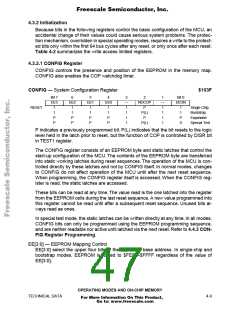
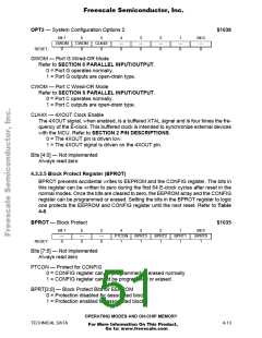
CONFIG — System Configuration Register
$103F
Bit 7
EE3
1
6
EE2
1
5
EE1
1
4
EE0
1
3
—
1
2
NOCOP
P
1
—
1
Bit 0
EEON
RESET:
1
1
P
0
Single Chip
Bootstrap
1
1
1
1
1
P(L)
P
1
P
P
P
P
1
1
Expanded
Special Test
P
P
P
P
1
P(L)
1
P indicates a previously programmed bit. P(L) indicates that the bit resets to the logic
level held in the latch prior to reset, but the function of COP is controlled by DISR bit
in TEST1 register.
The CONFIG register consists of an EEPROM byte and static latches that control the
start-up configuration of the MCU. The contents of the EEPROM byte are transferred
into static working latches during reset sequences. The operation of the MCU is con-
trolled directly by these latches and not by CONFIG itself. In normal modes, changes
to CONFIG do not affect operation of the MCU until after the next reset sequence.
When programming, the CONFIG register itself is accessed. When the CONFIG reg-
ister is read, the static latches are accessed.
These bits can be read at any time. The value read is the one latched into the register
from the EEPROM cells during the last reset sequence. A new value programmed into
this register cannot be read until after a subsequent reset sequence. Unused bits al-
ways read as ones.
In special test mode, the static latches can be written directly at any time. In all modes,
CONFIG bits can only be programmed using the EEPROM programming sequence,
and are neither readable nor active until latched via the next reset. Refer to 4.4.3 CON-
FIG Register Programming.
EE[3:0] — EEPROM Mapping Control
EE[3:0] select the upper four bits of the EEPROM base address. In single-chip and
bootstrap modes, EEPROM is forced to $FE00–$FFFF regardless of the value of
EE[3:0].
OPERATING MODES AND ON-CHIP MEMORY
TECHNICAL DATA
4-9
For More Information On This Product,
Go to: www.freescale.com

 FREESCALE [ Freescale ]