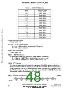
Freescale Semiconductor, Inc.
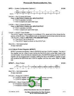
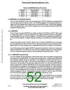
Table 4-6 EEPROM Block Protection
Bit Name
BPRT0
BPRT1
BPRT2
BPRT3
Block Protected
$xE00–$xE1F
$xE20–$xE5F
$xE60–$xEDF
$xEE0–$xFFF
Block Size
32 Bytes
64 Bytes
128 Bytes
288 Bytes
4.4 EEPROM and CONFIG Register
The 512-byte EEPROM array and the single-byte CONFIG register are implemented
with the same type of memory cells. The CONFIG register is a separate address lo-
cated within the register block rather than in the EEPROM array. Unlike other registers
within the register block, the CONFIG register can only be altered using the EEPROM
programming procedure.
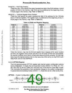
4.4.1 EEPROM
The 512-byte on-board EEPROM is initially located from $FE00 to $FFFF after reset
in single-chip modes. It can be mapped to any other 4-Kbyte boundary by program-
ming bits EE[3:0] in the CONFIG register. The EEPROM is enabled by the EEON bit
in the CONFIG register. Programming and erasing is controlled by the PPROG regis-
ter.
Unlike information stored in ROM, data in the 512 bytes of EEPROM can be erased
and reprogrammed under software control. Because programming and erasing oper-
ations use an on-chip charge pump, a separate external power supply is not required.
Use of the block protect register (BPROT) prevents inadvertent writes to (or erases of)
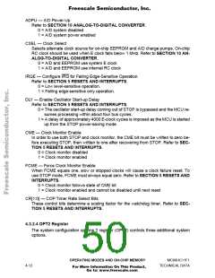
blocks of EEPROM. The CSEL bit in the OPTION register selects an on-chip oscillator
clock for programming and erasing while operating at frequencies below 1 MHz.
4.4.1.1 EEPROM Programming
An exact register access sequence must be followed to allow successful programming
and erasure of the EEPROM. The following procedures for modifying the EEPROM
and CONFIG register detail the sequence. If an attempt is made to set both EELAT
and EEPGM bits in the same write cycle and this attempt occurs before the required
write cycle with the EELAT bit set, then neither bit is set. If a write to an EEPROM ad-
dress is performed while the EEPGM bit is set, the write is ignored, and the program-
ming operation in progress is not disturbed. If no EEPROM address is written between
the point at which EELAT is set and EEPGM is set, then no program or erase operation
occurs. These safeguards are included to prevent accidental EEPROM changes in
cases of program runaway. If the frequency of the E clock is 1 MHz or less, the CSEL
bit in the OPTION register must be set to select the internal RC clock.
When the EELAT bit in the PPROG register is cleared, the EEPROM can be read as
if it were a ROM. The block protect register has no effect during reads. During EE-
PROM programming, the ROW and BYTE bits of PPROG are not used.
OPERATING MODES AND ON-CHIP MEMORY
MC68HC11F1
4-14
TECHNICAL DATA
For More Information On This Product,
Go to: www.freescale.com

 FREESCALE [ Freescale ]