Clock Generator Module (CGM)
the AUTO bit in the PLL bandwidth control register (PBWC) is clear. Clear the
PLLF bit by reading the PLL control register. Reset clears the PLLF bit.
1 = Change in lock condition
0 = No change in lock condition
NOTE:
Do not inadvertently clear the PLLF bit. Any read or read-modify-write operation on
the PLL control register clears the PLLF bit.
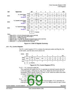
PLLON — PLL On Bit
This read/write bit activates the PLL and enables the VCO clock, CGMVCLK.
PLLON cannot be cleared if the VCO clock is driving the base clock, CGMOUT
(BCS = 1). See 4.3.3 Base Clock Selector Circuit. Reset sets this bit so that
the loop can stabilize as the MCU is powering up.
1 = PLL on
0 = PLL off
BCS — Base Clock Select Bit
This read/write bit selects either the crystal oscillator output, CGMXCLK, or the
VCO clock, CGMVCLK, as the source of the CGM output, CGMOUT. CGMOUT
frequency is one-half the frequency of the selected clock. BCS cannot be set
while the PLLON bit is clear. After toggling BCS, it may take up to three
CGMXCLK and three CGMVCLK cycles to complete the transition from one
source clock to the other. During the transition, CGMOUT is held in stasis. See
4.3.3 Base Clock Selector Circuit. Reset clears the BCS bit.
1 = CGMVCLK divided by two drives CGMOUT
0 = CGMXCLK divided by two drives CGMOUT
NOTE:
PLLON and BCS have built-in protection that prevents the base clock selector
circuit from selecting the VCO clock as the source of the base clock if the PLL is
off. Therefore, PLLON cannot be cleared when BCS is set, and BCS cannot be set
when PLLON is clear. If the PLL is off (PLLON = 0), selecting CGMVCLK requires
two writes to the PLL control register. See 4.3.3 Base Clock Selector Circuit.
PCTL[3:0] — Unimplemented Bits
These bits provide no function and always read as logic 1s.
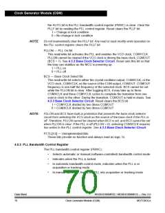
4.5.2 PLL Bandwidth Control Register
The PLL bandwidth control register (PBWC):
•
•
•
Selects automatic or manual (software-controlled) bandwidth control mode
Indicates when the PLL is locked
In automatic bandwidth control mode, indicates when the PLL is in
acquisition or tracking mode
•
In manual operation, forces the PLL into acquisition or tracking mode
Data Sheet
70
MC68HC908MR32 • MC68HC908MR16 — Rev. 6.0
Clock Generator Module (CGM)
MOTOROLA

 FREESCALE [ Freescale ]