Clock Generator Module (CGM)
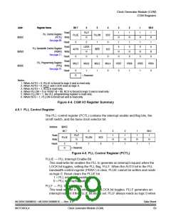
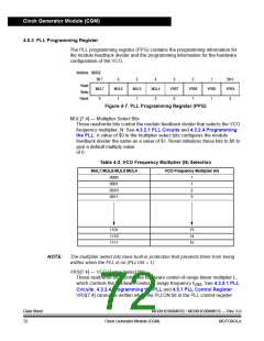
4.5.3 PLL Programming Register
The PLL programming register (PPG) contains the programming information for
the modulo feedback divider and the programming information for the hardware
configuration of the VCO.
Address: $005E
Bit 7
MUL7
0
6
MUL6
1
5
MUL5
1
4
MUL4
0
3
VRS7
0
2
VRS6
1
1
VRS5
1
Bit 0
VRS4
0
Read:
Write:
Reset:
Figure 4-7. PLL Programming Register (PPG)
MUL[7:4] — Multiplier Select Bits
These read/write bits control the modulo feedback divider that selects the VCO
frequency multiplier, N. See 4.3.2.1 PLL Circuits and 4.3.2.4 Programming
the PLL. A value of $0 in the multiplier select bits configures the modulo
feedback divider the same as a value of $1. Reset initializes these bits to $6 to
give a default multiply value
of 6.
Table 4-2. VCO Frequency Multiplier (N) Selection
MUL7:MUL6:MUL5:MUL4
VCO Frequency Multiplier (N)
0000
0001
0010
0011
1
1
2
3
1101
1110
1111
13
14
15
NOTE:
The multiplier select bits have built-in protection that prevents them from being
written when the PLL is on (PLLON = 1).
VRS[7:4] — VCO Range Select Bits
These read/write bits control the hardware center-of-range linear multiplier L,
which controls the hardware center-of-range frequency fVRS. See 4.3.2.1 PLL
Circuits, 4.3.2.4 Programming the PLL and 4.5.1 PLL Control Register.
VRS[7:4] cannot be written when the PLLON bit in the PLL control register
Data Sheet
72
MC68HC908MR32 • MC68HC908MR16 — Rev. 6.0
Clock Generator Module (CGM)
MOTOROLA

 FREESCALE [ Freescale ]